
Phase change memory materials, devices and methods
a technology of phase change memory and material, applied in the field of phase change memories, to achieve the effect of reducing the amount of energy necessary for nucleation, reducing the crystallisation energy of phase change material, and increasing the erasability of recording medium
- Summary
- Abstract
- Description
- Claims
- Application Information
AI Technical Summary
Benefits of technology
Problems solved by technology
Method used
Image

Examples
example 1
Operation of GLS Phase Alloy
[0112] In this example, we demonstrate electrical phase change behaviour of a thin film GLS alloy. The phase-change alloy comprises Ga, La, and S in which the ratio of Ga to La to S (Ga:La:S) is chosen as approximately 1:3:6 to form a phase change alloy. More preferably, the electrical phase-change alloy comprises Ga, La, S in the ratio Gaw Lax Sy where 5<w<10, 25<x<35, 50<y<70. More preferably, w+x+y=100%. More preferably, the ratio of both Ga atoms to S atoms and La atoms to sulphur atoms is chosen as 2:3 and the ratio of 2Ga:3S to 2La:3S is chosen to be 1:3.
[0113] In one embodiment of the present invention, the means for delivering is a first contact and a second contact. Each of the contacts is adjoining the volume of memory material. As used herein, a contact is adjoining the volume of memory material if at least a portion of the contact is touching the memory material.
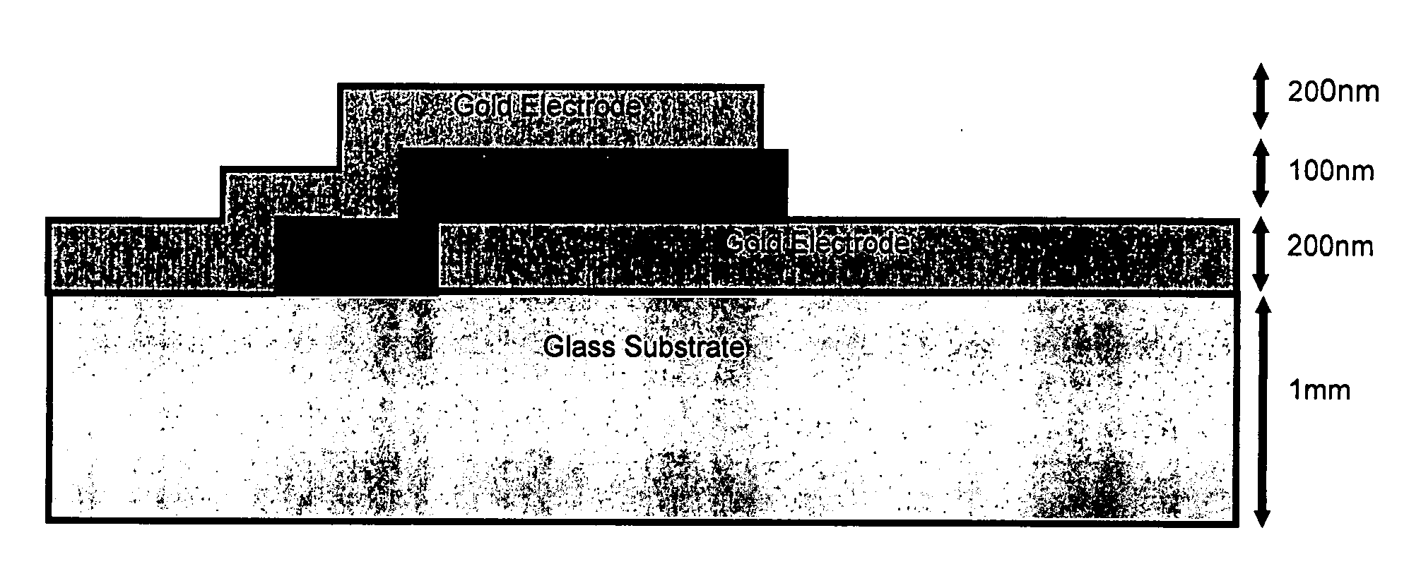
[0114] A borosilicate microscope slide was used as a substrate on which the pha...
example 2
Electrical Phase Change Memory Cell Array
[0118] In this example we demonstrate the operation of our GLS phase change alloy as an electrical data storage element. We demonstrate electrical phase change behaviour of an array of memory cells fabricated from a range of GLS alloy compositions. The phase-change alloy comprises Ga, La, and S in which the Ga to La to S ratio is chosen to vary over a wide range. Here the phase-change alloy comprises Ga, La, S in the ratio Gaw Lax Sy where 5
[0119] As in the previous example, metallic tracks were thermally evaporated onto a suitable substrate using an Edwards coater. The tracks were fabricated from Chromium since its melting point (1907° C.) is far greater than that of the aforementioned GLS phase change alloy. The tracks were typically 1 mm width, 200 nm depth and 50 mm length. The phase change alloy GLS was then deposited by pulse laser deposition onto the surface electrodes and substrate. The substr...
example 3
GLS Alloy Optimisation
[0126] In order to optimise the Ga:La:S glass system for phase change applications, an experimental study was made to analyse the crystallisation kinetics of a series of glasses with varying Ga to La ratio. Small deviations from the eutectic composition cause a great increase in the crystallisation time. At the eutectic composition it is possible to crystallise traditional phase change materials in just 30 ns, but if one deviates from this eutectic by only 10% the crystallisation time increases to over 1 μs. This underlies the need to design a phase change material at the eutectic composition.
[0127] Early studies to measure the eutectic of Ga:La:S based glasses were flawed due to the lack of phase-pure raw materials, in particular phase-pure gallium sulphide. To avoid this problem, phase-pure materials were synthesised and verified using the method described in U.S. Pat. No. 6,803,335 [79].
[0128] The synthesis of phase-pure GaS was achieved by batching equal...
PUM
 Abstract
Description
Claims
Application Information