Light emitting element and light emitting device

Active Publication Date: 2007-08-09
SEMICON ENERGY LAB CO LTD
View PDF25 Cites 25 Cited by
  • Summary
  • Abstract
  • Description
  • Claims
  • Application Information

AI Technical Summary

Benefits of technology

[0010] In another aspect of the invention, a light emitting element includes n pieces of light emitting layers (n is a natural number) between a first electrode and a second electrode. The second electrode reflects light more easily as compared with the first electrode. The light emitting element further includes a first layer and a second layer between the mth light emitting layer (m is a natural number: 1=m=n) and the m+1th light emitting layer. Further, the first and second layers are contacted to each other. The first layer includes a substance that transports holes easily and a layer with an electron accepting property. The second layer includes a substance that transports electrons easily and a substance with an electron donating property. The m+1th light emitting layer exhibits a shorter peak wavelength of emission spectrum than that of the mth light emitting layer. The n pieces of light emitting layers are provided such that the m+1th light emitting layer is placed closer to the second electrode than the mth light emitting layer.
[0011] In another aspect of the invention, a light emitting element includes n pieces of light emitting layers (n is a natural number) between a first electrode and a second electrode. The second electrode reflects light more

Problems solved by technology

Therefore, the light emitting element is possibly deteriorated due to moisture absorbed by vanadium pentoxide.
The

Method used


Image

  • Light emitting element and light emitting device
  • Light emitting element and light emitting device
  • Light emitting element and light emitting device

Examples


embodiment mode 1

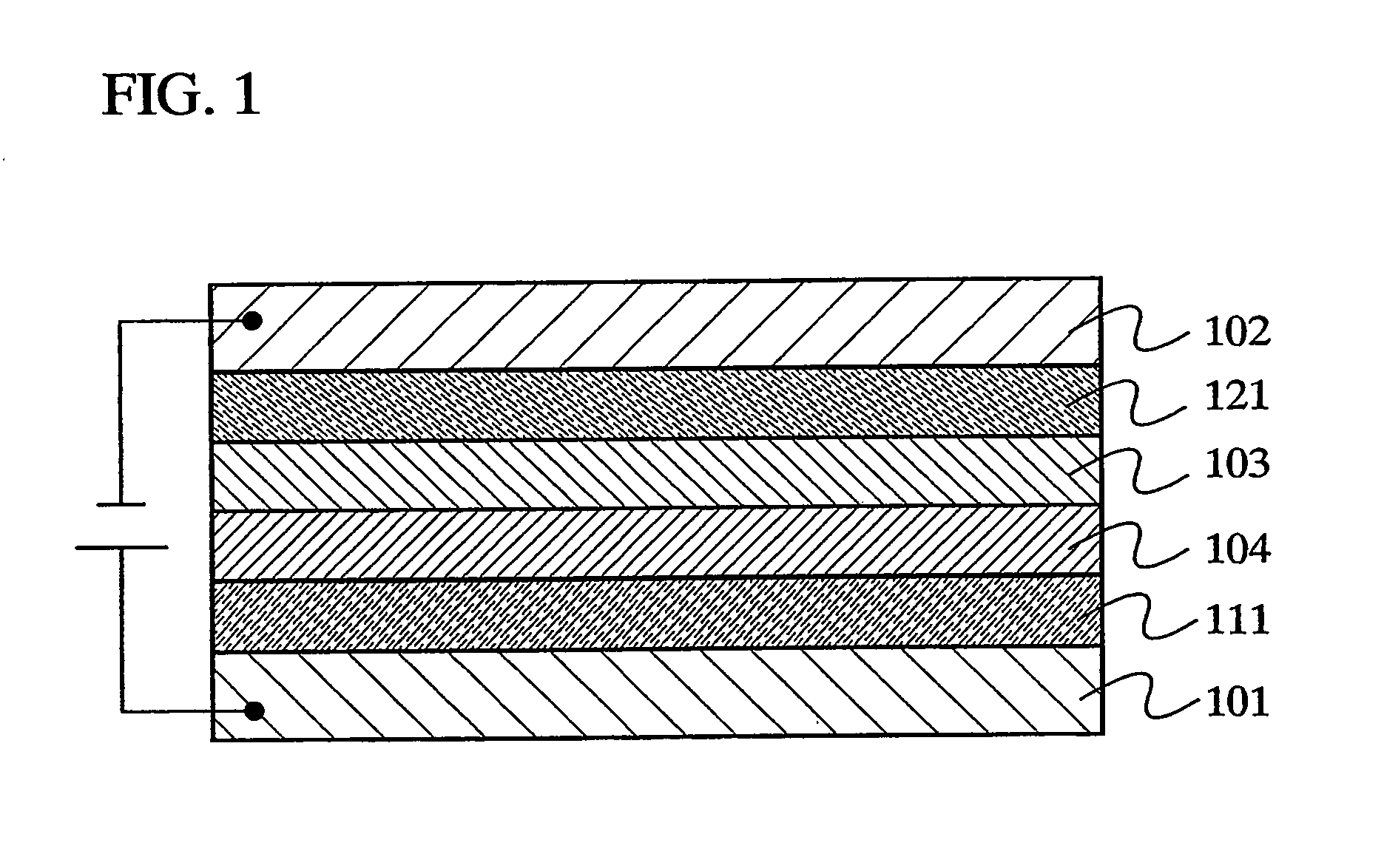
[0025] In FIG. 1, a first layer 103 containing a substance that transports holes easily and a substance with an electron accepting property and a second layer 104 containing a substance that transports electrons easily and a substance with an electron donating property are provided between a first electrode 101 and a second electrode 102. The first layer 103 and the second layer 104 are laminated in contact with each other. Further, holes are generated in the first layer 103 containing the substance that transports holes easily and the substance with the electron accepting property whereas electrons are generated in the second layer 104 containing the substance that transports electrons easily and the substance with the electron donating property.

[0026] Also, a first light emitting layer 111 is provided between the first electrode 101 and the first layer 103. A second light emitting layer 121 is provided between the second electrode 102 and the second layer 104.

[0027] Further, in ...

embodiment mode 2

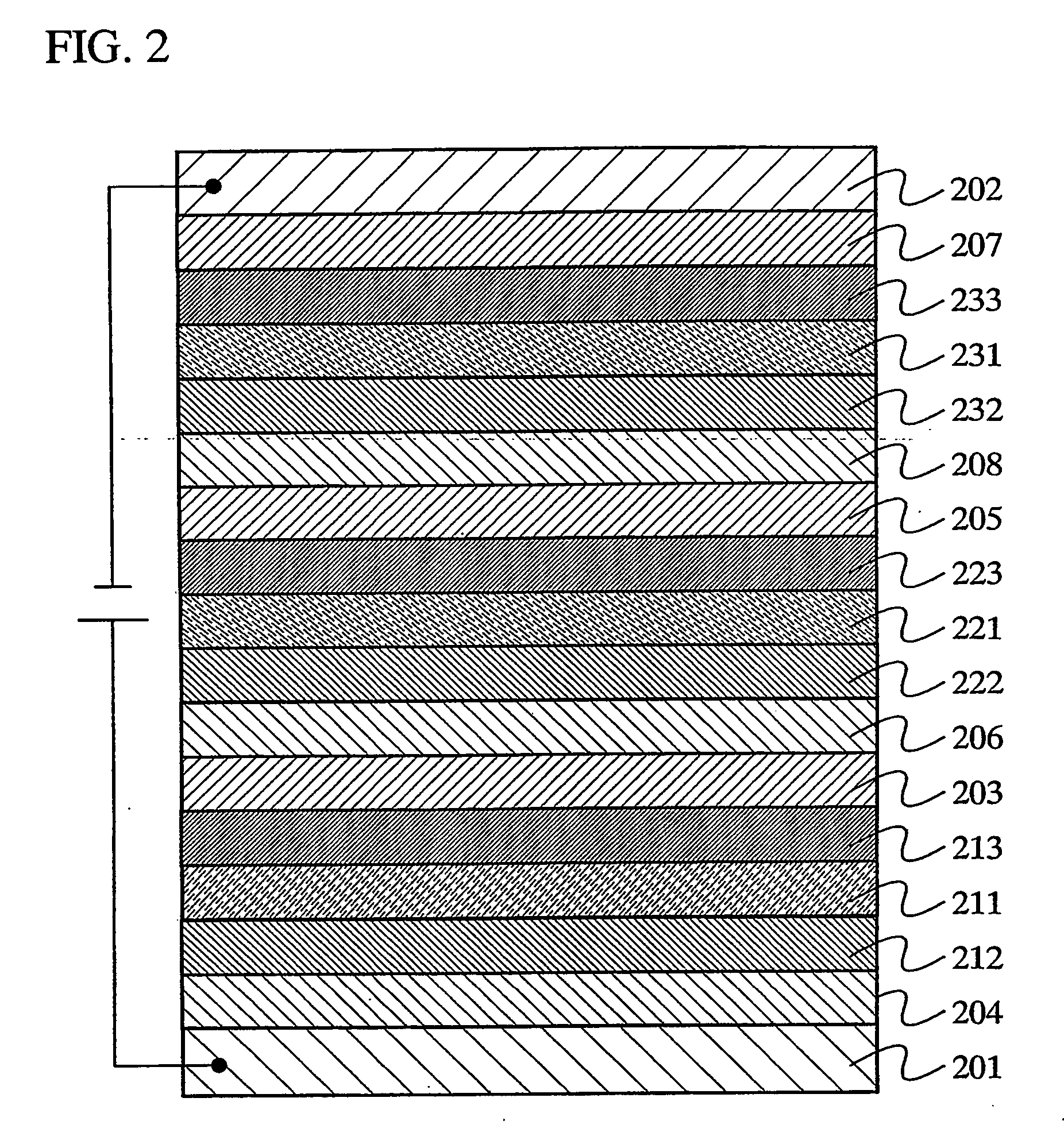
[0040] The present embodiment mode will describe a light emitting element of the invention including three light emitting layers with reference to FIG. 2.

[0041] In FIG. 2, first layers 203, 205 and 207 including a substance that transports electrons easily and a substance with an electron donating property, and second layers 204, 206 and 208 including a substance that transports holes easily and a substance with an electron accepting property are provided between a first electrode 201 and a second electrode 202. In this case, the first layer 203 is formed in contact with the first electrode 201. The second layer 208 is formed in contact with the second electrode 202. The first layer 205 and the second layer 204 are laminated to be in contact with each other. The first layer 207 and the second layer 206 are laminated to be in contact with each other. Holes are generated in the first layers 203, 205 and 207 including the substance that transports holes easily and the substance with t...

embodiment mode 3

[0050] The light emitting element of the invention as described in Embodiment Mode 1 or 2 can be applied to a pixel portion of a light emitting device having a display function or a lighting portion of a light emitting device having a lighting function.

[0051] The present embodiment mode will describe a circuit configuration of a light emitting device having a display function and a method for driving thereof with reference to FIGS. 3 to 6.

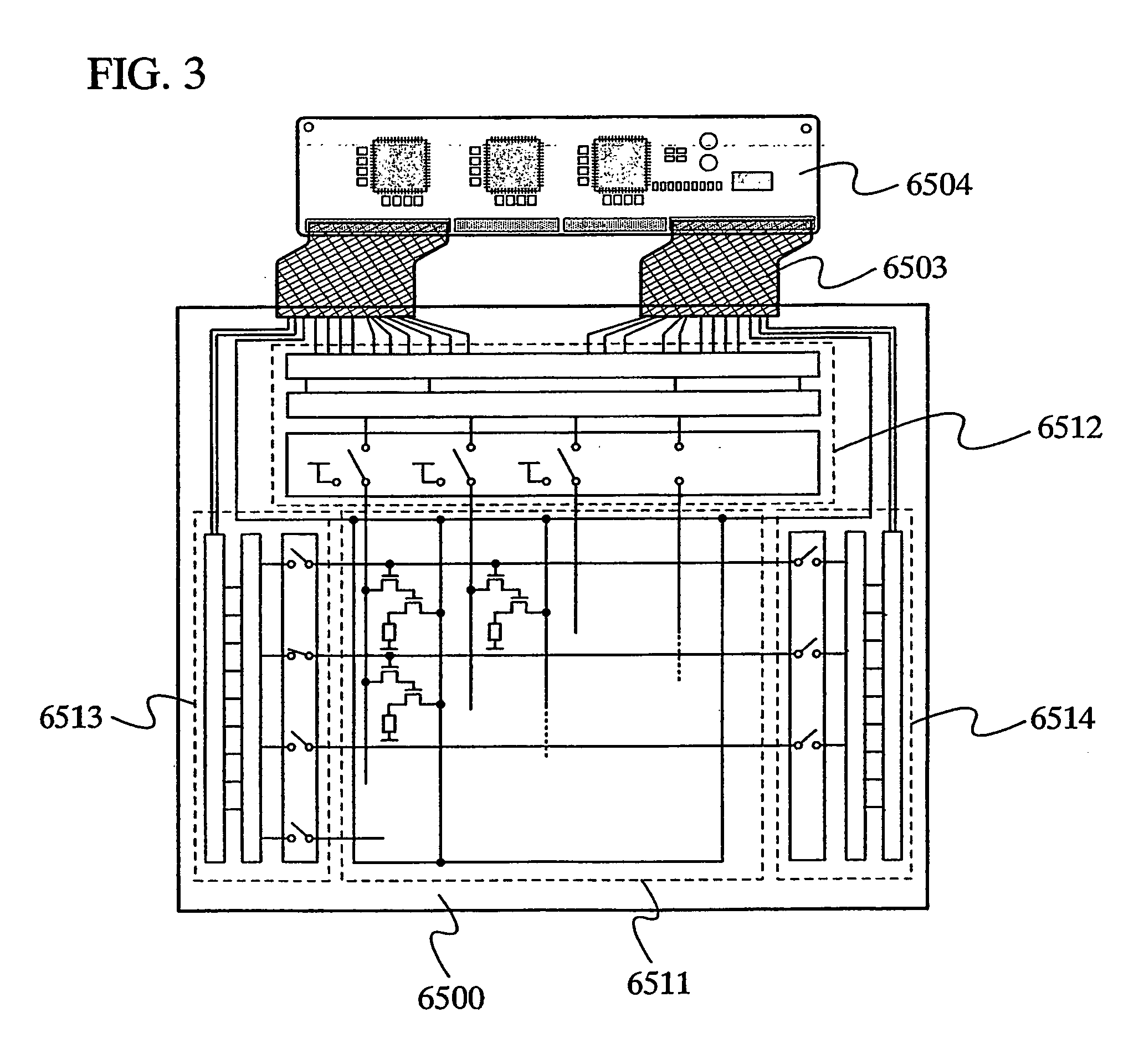
[0052]FIG. 3 is a schematic view seen from a top face of the light emitting device according to the invention. In FIG. 3, a pixel portion 6511, a source signal line driver circuit 6512, a writing gate signal line driver circuit 6513 and an erasing gate signal line driver circuit 6514 are provided over a substrate 6500. The source signal line driver circuit 6512, the writing gate signal line driver circuit 6513 and the erasing gate signal line driver circuit 6514 are connected to FPCs (flexible printed circuits) 6503 that are external input termin...


PUM

PropertyMeasurementUnit
Lengthaaaaaaaaaa
Wavelengthaaaaaaaaaa
Reflectanceaaaaaaaaaa

Abstract

A light emitting element of the invention includes n pieces of light emitting layers (n is a natural number) between first and second electrodes. A first layer and a second layer are provided between the mth light emitting layer (m is a natural number of 1≦m≦n) and the m+1th light emitting layer. The first and second layers are contacted to each other. The first layer contains a substance that transports holes easily and a substance with an electron accepting property. The second layer contains a substance that transports electrons easily and a substance with an electron donating property. Molybdenum oxide is used as the substance with the electron accepting property.

Description

TECHNICAL FIELD [0001] The present invention relates to a light emitting element having a light emitting layer between a pair of electrodes, and in particular, relates to a layer structure of the light emitting element. BACKGROUND ART [0002] A light emitting device utilizing light emitted from an electroluminescent element (a light emitting element) has wide-viewing angle and low power consumption. In recent years, research and development of a light emitting device, which can provide high quality images for the long term, have been carried out actively in the development area of light emitting devices so as to dominate the market for display devices that are applied to various kinds of information processing devices such as a television receiver and a car navigation system. [0003] In order to obtain a light emitting device, which can provide high quality images for the long term, development of a long-life light emitting element and a light emitting element that emits light efficie...

Claims


Application Information

Patent Timeline
IPC IPC(8): H01L51/52H05B44/00H01L27/32H01L51/50H05B33/12H05B33/14H05B33/22
CPCH01L27/3209H01L51/5048H01L51/5278Y10T428/24942H01L51/5237Y10S428/917H01L27/3241H10K59/32H10K59/12H10K50/155H10K50/165H10K50/84H10K50/19H10K50/15C09K15/02C01G39/02C01G39/00Y02B20/30H10K2102/301H10K59/10H10K50/14
Inventor KUMAKI, DAISUKEIKEDA, HISAOABE, HIROKOSEO, SATOSHI
Owner SEMICON ENERGY LAB CO LTD
Why Eureka
Try Eureka