Manufacturing method of memory element, laser irradiation apparatus, and laser irradiation method

Active Publication Date: 2007-08-09
SEMICON ENERGY LAB CO LTD
View PDF25 Cites 15 Cited by
  • Summary
  • Abstract
  • Description
  • Claims
  • Application Information

AI Technical Summary

Benefits of technology

[0022]In the present invention, with the use of a diffractive optical element and a deflector in combination, laser irradiation can be performed as various irradiation patterns are switched. In addition, a plurality of beam spots can be formed at a time and laser beam irradiation can be performed efficiently. Further, since a traveling direction of a laser beam can be controlled

Problems solved by technology

In the case where it is desired to perform laser irradiation with various patterns in such a manner, in the laser processing apparatus of Patent Document 1, it has been difficult to allocate an ID for each ROM because there is no function of isolating each irradiation pattern.
Naturally, it is necessary to separately use a mask in order to allocate various IDs even in

Method used


Image

  • Manufacturing method of memory element, laser irradiation apparatus, and laser irradiation method
  • Manufacturing method of memory element, laser irradiation apparatus, and laser irradiation method
  • Manufacturing method of memory element, laser irradiation apparatus, and laser irradiation method

Examples


embodiment mode 1

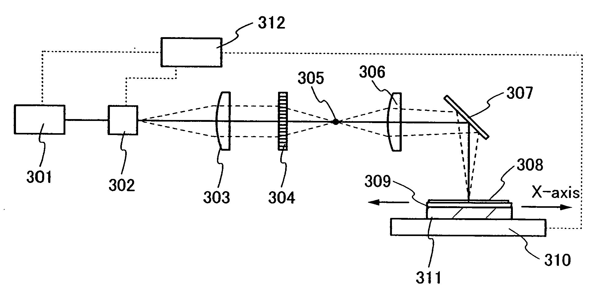
[0049]This embodiment mode will explain a structure of an apparatus for rapidly performing laser irradiation in a desired position as laser irradiation patterns are switched and a laser irradiation method with reference to FIGS. 1A and 1B, FIG. 2, FIG. 3, and FIG. 4.

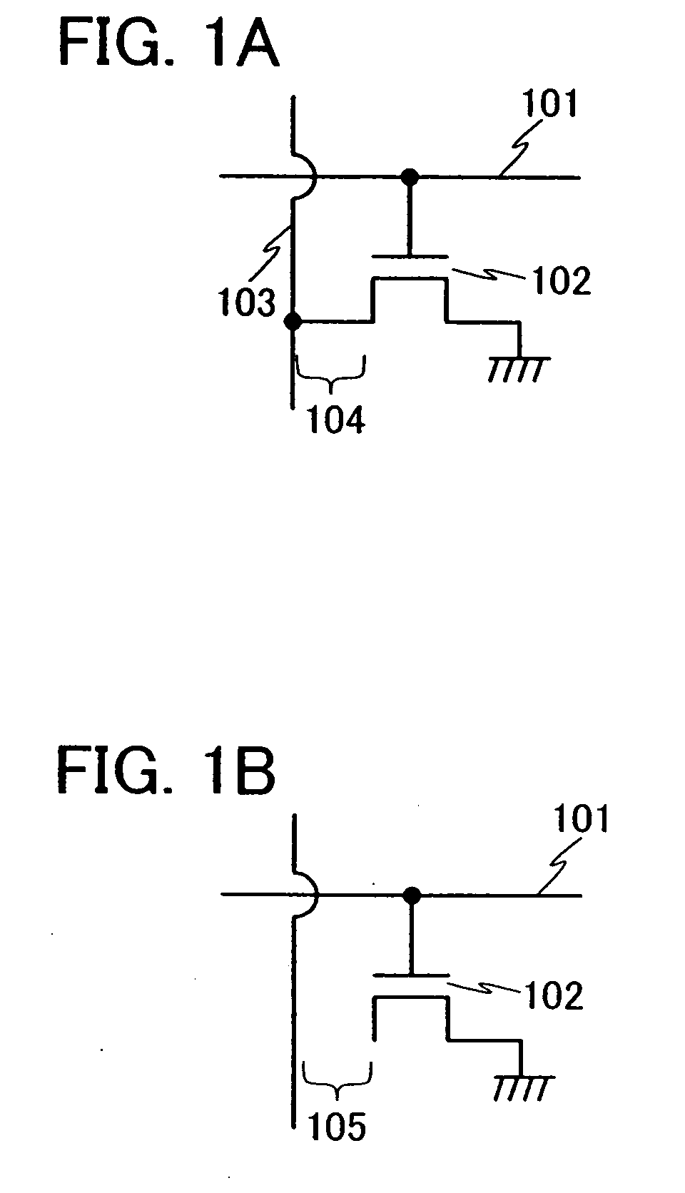
[0050]In a case of manufacturing a ROM, information is stored by change of a wiring method of a transistor in order to distinguish pieces of binary information of “0” and “1”. FIGS. 1A and 1B each show an example of a circuit configuration of a memory cell where contact writing is performed. FIG. 1A is a circuit configuration for holding “0” of the pieces of binary information. In this configuration, a transistor 102 is connected to a word line 101 for driving the memory cell and a bit line 103. Here, the connection to the bit line is performed by a wiring formed in a region 104. On the other hand, FIG. 1B is a circuit configuration for holding “1” of the pieces of the binary information. In this configuration, a transis...

embodiment mode 2

[0064]This embodiment mode will explain a laser irradiation apparatus by division of a laser beam with the use of a reflection-type diffractive optical element and a laser irradiation method.

[0065]FIG. 5 shows a block diagram of a laser irradiation apparatus of this embodiment mode. A laser beam emitted from a laser oscillator 401 passes through a deflector 402. This embodiment mode will show an example where an AOD (Acousto-Optical Deflector) is used as the deflector 402. Note that the deflector that is used in the present invention is not limited to an AOD. For example, a galvanometer mirror may be used to control the traveling direction of the laser beam. An AOD is a deflector for deflecting a laser beam by an acoustooptic effect in an optical medium. A laser beam that is deflected at a deflection angle in proportion to an acoustic wave frequency added to the AOD enters a reflection-type diffractive optical element 403. The reflection-type diffractive optical element 403 is desig...

embodiment mode 3

[0072]This embodiment mode will explain a laser irradiation apparatus, where a plurality of optical systems that can form various irradiation patterns is disposed so that a plurality of irradiation points can be irradiated efficiently with laser beams, and a laser irradiation method.

[0073]FIG. 7 shows a perspective view of a laser irradiation apparatus of this embodiment mode. In the laser irradiation apparatus shown in FIG. 7, four sets of optical systems are provided on an element mounting base 510. In this embodiment mode, a set of optical systems includes a laser oscillator 501, a deflector 502, a collimating lens 503, a transmission type diffractive optical element 504, a mirror 505, and a projection lens 506. A laser beam emitted from the laser oscillator 501 passes through the deflector 502. This embodiment mode will show an example where an AOD (Acousto-Optical Deflector) is used as the deflector 502. Note that the deflector that is used in the present invention is not limit...


PUM

PropertyMeasurementUnit
Transmissionaaaaaaaaaa

Abstract

A method for rapidly performing laser irradiation in a desired position as laser irradiation patterns are switched is proposed. A laser beam emitted from a laser oscillator is entered into a deflector, and a laser beam which has passed through the deflector is entered into a diffractive optical element to be diverged into a plurality of laser beams. Then, a photoresist formed over an insulating film is irradiated with the laser beam which is made to diverge into the plurality of laser beams, and the photoresist irradiated with the laser beam is developed so as to selectively etch the insulating film.

Description

TECHNICAL FIELD[0001]The present invention relates to a laser irradiation apparatus for efficiently performing laser irradiation which is performed by a laser direct drawing method or the like and a laser irradiation method. In addition, the present invention relates to a manufacturing method of a memory element including the laser irradiation step.BACKGROUND ART[0002]In a manufacturing process of a semiconductor, a manufacturing process of a printed wiring board, or the like, microfabrication is required due to the integration of a circuit. In general, a photomask where a circuit pattern is written is manufactured beforehand and a laser light-exposure technique for transferring the pattern to a substrate is used to perform such microfabrication. However, with a method of using a photomask, it takes cost and time to manufacture a mask. Therefore, in recent years, a mask-less process has drawn attention. There is a laser direct drawing method as a typical mask-less process. By the la...

Claims


Application Information

Patent Timeline
IPC IPC(8): H01L21/20
CPCB23K26/0656B23K26/067B23K26/0676G03F7/70316G03F7/70383H01L27/13H01L21/84H01L27/11226H01L27/11293H01L27/1214H01L27/1266H01L21/31144B23K26/066H10B20/34H10B20/65
Inventor TANAKA, KOICHIROOISHI, HIROTADA
Owner SEMICON ENERGY LAB CO LTD
Why Eureka
Try Eureka