Copper Interconnect Wiring and Method and Apparatus for Forming Thereof

a technology of copper interconnect wires and wires, applied in the direction of vacuum evaporation coatings, solid-state devices, coatings, etc., can solve the problems of interconnection wires failing, copper wire surface, and the need to carry ever-higher electrical currents in smaller and smaller sizes

Inactive Publication Date: 2007-08-09
TEL EPION
View PDF33 Cites 34 Cited by
  • Summary
  • Abstract
  • Description
  • Claims
  • Application Information

AI Technical Summary

Benefits of technology

[0024] Still another embodiment of the present invention provides a method of forming a copper capping structure on an integrated circuit interconnection layer including one or more copper interconnect surfaces and one or more dielectric layer regions covered by barrier layer material, and may comprise the steps of: forming at least one capping structure on the one or more copper interconnect surfaces; and after forming the at least one capping structure on the one or more copper interconnect surfaces, removing the barrier layer material covering at least one of the one or more dielectric layer regions. The forming step may further comprise forming an accelerated capping GCIB and directing the accelerated capping GCIB onto at least one of the one or more copper interconnect surfaces. The removing step may comprise forming an accelerated etching GCIB and directing the accelerated etching GCIB onto the barrier layer material.
[0025] Even another embodiment of the present invention provides a method of forming a copper capping structure on an integrated circuit interconnection layer including one or more copper interconnect surfaces and one or more dielectric layer regions covered by barrier layer material, and the method may comprise the steps of: forming an accelerated capping GCIB using a first beam acceleration potential; directing the accelerated capping GCIB onto at least one of the one or more copper interconnect surfaces to form at least one capping structure on the one or more copper interconnect surfaces; forming an accelerated etching GCIB using a second beam acceleration

Problems solved by technology

However, a problem resulting from this scaling is the requirement to carry ever-higher electrical currents in smaller and smaller interconnection wires.
When the current densities and temperatures in such small wires get too high, the interconnect wires can fail by a phenomenon called electromigration.
The effects of the so-called “electron wind” that occurs in high current-density interconnect wires causes metal atoms to be swept away from their original lattice positions, resulting in either an open circuit in the wire or an extrusion short in an area where these diffusing metal atoms collect.
Unfortunately, these PECVD deposited capping materials form a defective interface with the copper that results in enhanced copper migration along the top surface of the copper wire and therefore higher electromigration failure rates.
Unfortunately, all of the methods that use a selective metallic capping solution have some probability of also depositing some metal on the adjacent insulator surface and therefore causing unintended Leakage or shorts between adjacent metal lines.
In this prior art wiring scheme, it is along th

Method used


Image

  • Copper Interconnect Wiring and Method and Apparatus for Forming Thereof
  • Copper Interconnect Wiring and Method and Apparatus for Forming Thereof
  • Copper Interconnect Wiring and Method and Apparatus for Forming Thereof

Examples


first embodiment

[0046]FIG. 4A is a schematic showing a wiring scheme 500 of a copper interconnect capped using GCIB infusion according to the invention (showing for example, not for limitation, two copper wire layer interconnect levels). The schematic shows a substrate 501 supporting a first copper wire layer 502, a second copper wire layer 504, and copper via structure 506 connecting the two copper layers, each of which may be formed using conventional techniques. The substrate 501 is typically a semiconductor substrate containing active and / or passive elements (possibly including lower interconnect levels) requiring electrical interconnection. The sidewalls and bottoms of both copper wire layers 502 and 504 and the via structure 506 are lined with a TaN / Ta or other conventional barrier layer 512, which may be formed using conventional techniques. First inter-level dielectric layer 508 and second inter-level dielectric layer 510 provide electrical insulation between the copper wire layers and othe...

third embodiment

[0064]FIG. 6A is a schematic showing a wiring scheme 700 of a copper interconnect capped using GCIB infusion according to the invention (showing for example, not for limitation, two copper wire layer interconnect levels). The schematic shows a substrate 701 supporting a first copper wire layer 702, a second copper wire layer 704, and copper via structure 706 connecting the two copper layers, each of which may be formed using conventional techniques. The substrate 701 is typically a semiconductor substrate containing active and / or passive elements (possibly including lower interconnect levels) requiring electrical interconnection. The sidewalls and bottoms of both copper wire layers 702 and 704 and the via structure 706 are lined with a barrier layer 712, which may be formed using conventional techniques. First inter-level dielectric layer 708 and second inter-level dielectric layer 710 provide electrical insulation between copper wires and may be formed using conventional techniques...

fourth embodiment

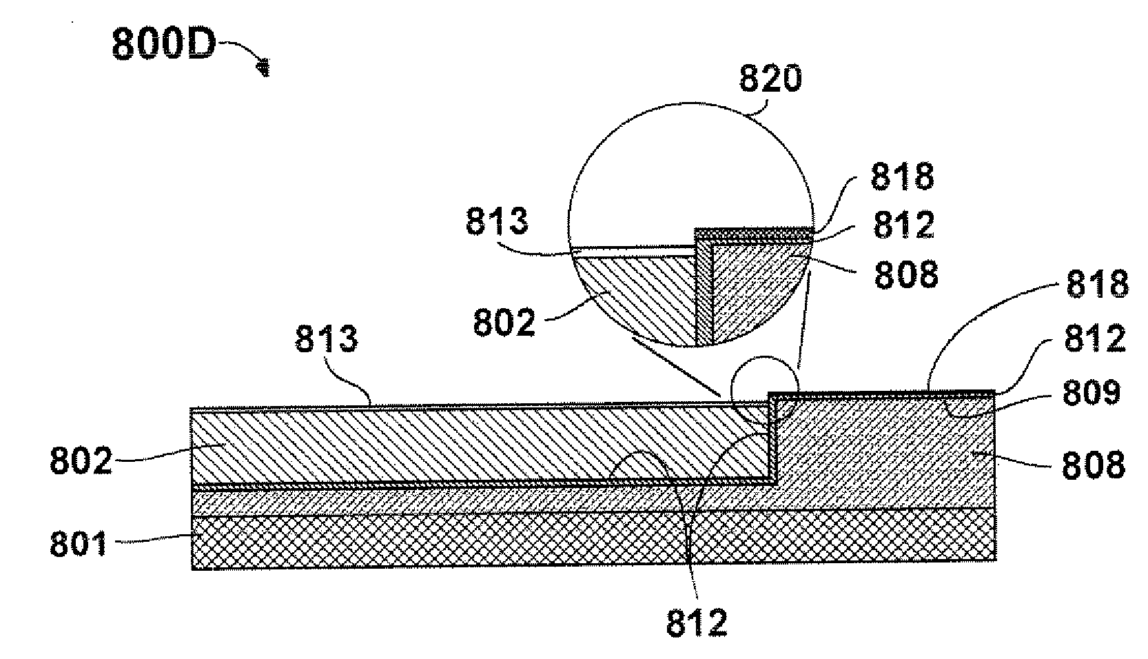
[0072]FIG. 7A is a schematic showing a wiring scheme 800 of a copper interconnect capped using GCIB infusion according to the invention (showing for example, not for limitation, two copper wire layer interconnect levels). The schematic shows a substrate 801 supporting a first copper wire layer 802, a second copper wire layer 804, and copper via structure 806 connecting the two copper layers, each of which may be formed using conventional techniques. The substrate 801 is typically a semiconductor substrate containing active and / or passive elements (possibly including lower interconnect levels) requiring electrical interconnection. The sidewalls and bottoms of both copper wire layers 802 and 804 and the via structure 806 are lined with a barrier layer 812, which may be formed using conventional techniques. First inter-level dielectric layer 808 and second inter-level dielectric layer 810 provide electrical insulation between copper wires and maybe formed using conventional techniques....


PUM

PropertyMeasurementUnit
Electric potential / voltageaaaaaaaaaa
Thicknessaaaaaaaaaa

Abstract

Capping layer or layers on a surface of a copper interconnect wiring layer for use in interconnect structures for integrated circuits and methods and apparatus for forming improved integration interconnection structures for integrated circuits by the application of gas-cluster ion-beam processing. Reduced copper diffusion and improved electromigration lifetime result and the use of selective metal capping techniques and their attendant yield problems are avoided. Various cluster tool configurations including gas-cluster ion-beam processing modules for copper capping, cleaning, etching, and film formation steps are disclosed.

Description

CROSS-REFERENCE TO RELATED APPLICATIONS [0001] This application is a continuation-in-part application of U.S. patent application Ser. No. 11 / 269,382, filed 8 Nov., 2005, and titled “COPPER INTERCONNECT WIRING AND METHOD OF FORMING THEREOF”, which claims the benefit of priority to U.S. Provisional Application Ser. No. 60 / 625,831, filed 8 Nov., 2004, and titled “COPPER INTERCONNECT WIRING AND METHOD OF FORMING THEREOF”. This application further claims priority to U.S. Provisional Application Ser. No. 60 / 765,664, filed 6 Feb., 2006, and titled “COPPER INTERCONNECT WIRING AND METHOD OF FORMING THEREOF”. The contents of all of the aforementioned applications are hereby incorporated herein by reference as if laid out in their entirety.FIELD OF THE INVENTION [0002] This invention relates generally to capping layers on surfaces of copper interconnect wiring layers and to improved methods and apparatus for forming interconnect structures for semiconductor integrated circuits by the applicati...

Claims


Application Information

Patent Timeline
IPC IPC(8): H01L21/44
CPCC23C14/0605C23C14/0635H01L2924/0002C23C14/0652C23C14/221C23C16/26C23C16/325C23C16/345C23C16/513H01J2237/0812H01L21/02074H01L21/02301H01L21/02304H01L21/321H01L21/32136H01L21/67207H01L21/76801H01L21/76822H01L21/76825H01L21/76832H01L21/76834H01L21/76843H01L21/76846H01L21/76849H01L21/76865H01L21/76867H01L21/76883H01L21/76886H01L2924/00
Inventor LEARN, ARTHUR J.SHERMAN, STEVEN R.GEFFKEN, ROBERT MICHAELHAUTALA, JOHN J.
Owner TEL EPION
Why Eureka
Try Eureka