Semiconductor device and method of manufacturing the same

a technology of semiconductors and semiconductors, applied in the direction of transistors, television systems, radio controlled devices, etc., can solve the problems of difficult to ensure the fixing strength, parts may not be fixed firmly any more, and the stress is not alleviated flexibly, so as to reduce the area for mounting, reduce the volume of parts due, and reduce the cost

Inactive Publication Date: 2007-08-16
SEMICON ENERGY LAB CO LTD
View PDF21 Cites 29 Cited by
  • Summary
  • Abstract
  • Description
  • Claims
  • Application Information

AI Technical Summary

Benefits of technology

[0053] By forming a visible light sensor and an amplifier circuit comprising a TFT over the same substrate, it is possible to reduce the cost, the volume of the parts due to reduction in thickness, and the area for mounting, and besides, noise superposition can be reduced.
[0054] By forming a visible light sensor by a sensor element using an amorphous silicon film, an infrared light cut filter is not required and the visible light sensor can be a sensor element having a reduced output variation. Furthermore, output current can be increased and a variation can be suppressed by the amplifier circuit comprising a TFT formed over the same substrate as the visible light sensor. The light receiving area can be reduced because of output amplification by the amplifier circuit, thereby reduction in size and weight of a mounted set, and reduction of the number of components can be achieved.

Problems solved by technology

Therefore, in the case of mounting by soldering, for example, it is difficult to ensure the fixing strength.
In the case where a region for fixing is small and the degree of hardness of the sensor element (which means the mechanical strength of the single crystalline silicon substrate, the glass substrate, or the like) is high, when bending stress is applied to the parts, the stress is not alleviated flexibly and therefore the parts may not be fixed firmly any more because of balance between the fixing strength and the mechanical stress.

Method used


Image

  • Semiconductor device and method of manufacturing the same
  • Semiconductor device and method of manufacturing the same
  • Semiconductor device and method of manufacturing the same

Examples


embodiment mode 1

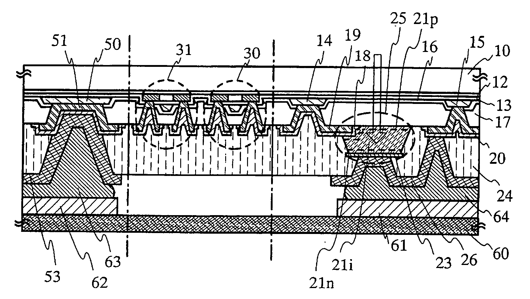
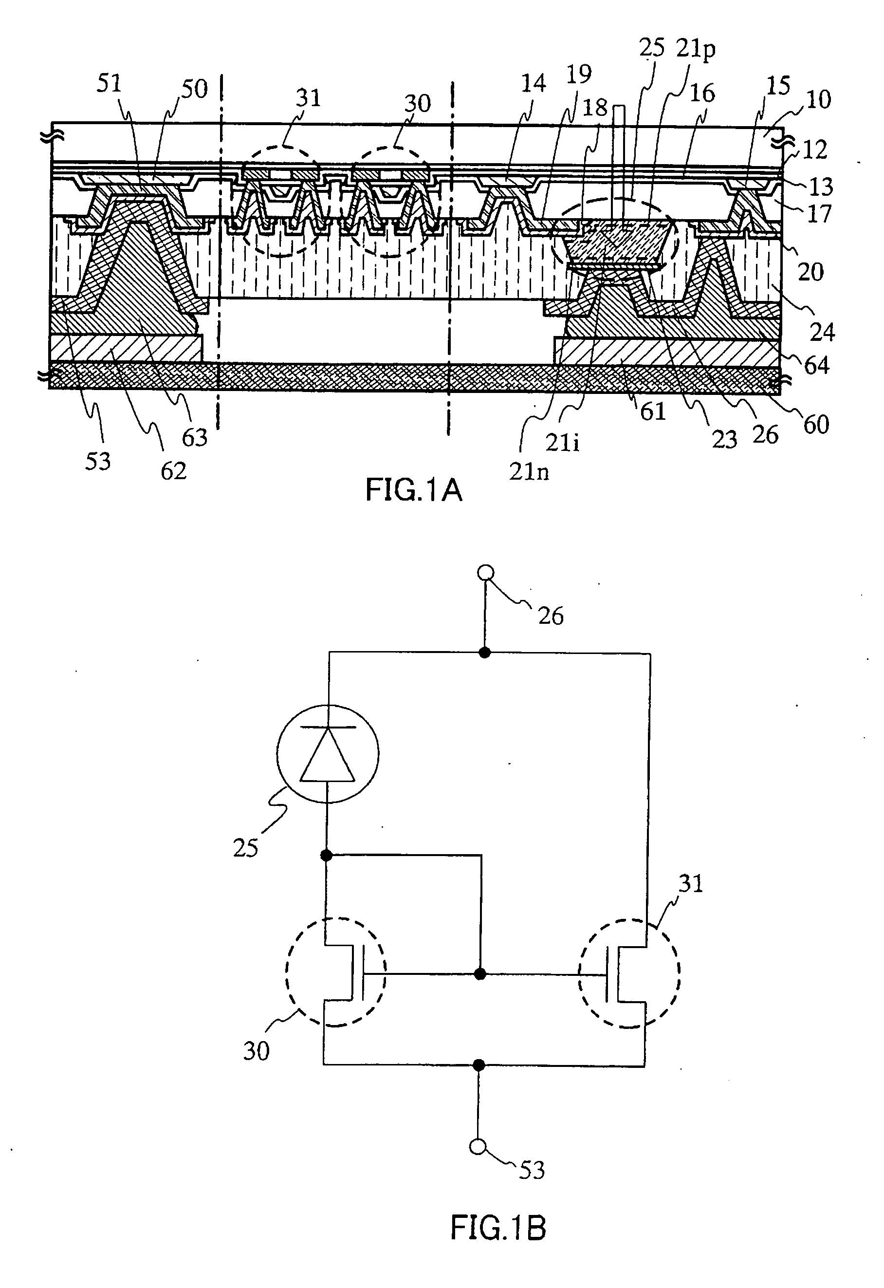
[0056]FIG. 1(A) is a cross-sectional view of a mounted light sensor chip of the present invention. FIG. 1A shows an example of a visible light sensor chip (2.0 mm×1.5 mm) having two terminals. In FIG. 1A, reference numeral 10 denotes a glass substrate, reference numeral 12 denotes a base insulating film, and reference numeral 13 denotes a gate insulating film. Since received light passes through the glass substrate 10, the base insulating film 12, and the gate insulating film 13, these are preferably formed of a material having high transmittance.

[0057] A PIN photodiode 25 is structured by a first electrode 18, a second electrode 23, a p-type semiconductor layer 21p, an n-type semiconductor layer 21n, and an i-type (intrinsic) semiconductor layer 21i sandwiched between the p-type semiconductor layer and the n-type semiconductor layer.

[0058] A wire 19 has a stacked layer structure of a high melting point metal film and a low resistance metal film (e.g., an aluminum alloy, pure alum...

embodiment mode 2

[0109] Described in this embodiment mode is a case where a part of the steps described in Embodiment Mode 1 is performed by screen printing. As for the same step as that of Embodiment Mode 1, specific description thereof is omitted for simplicity.

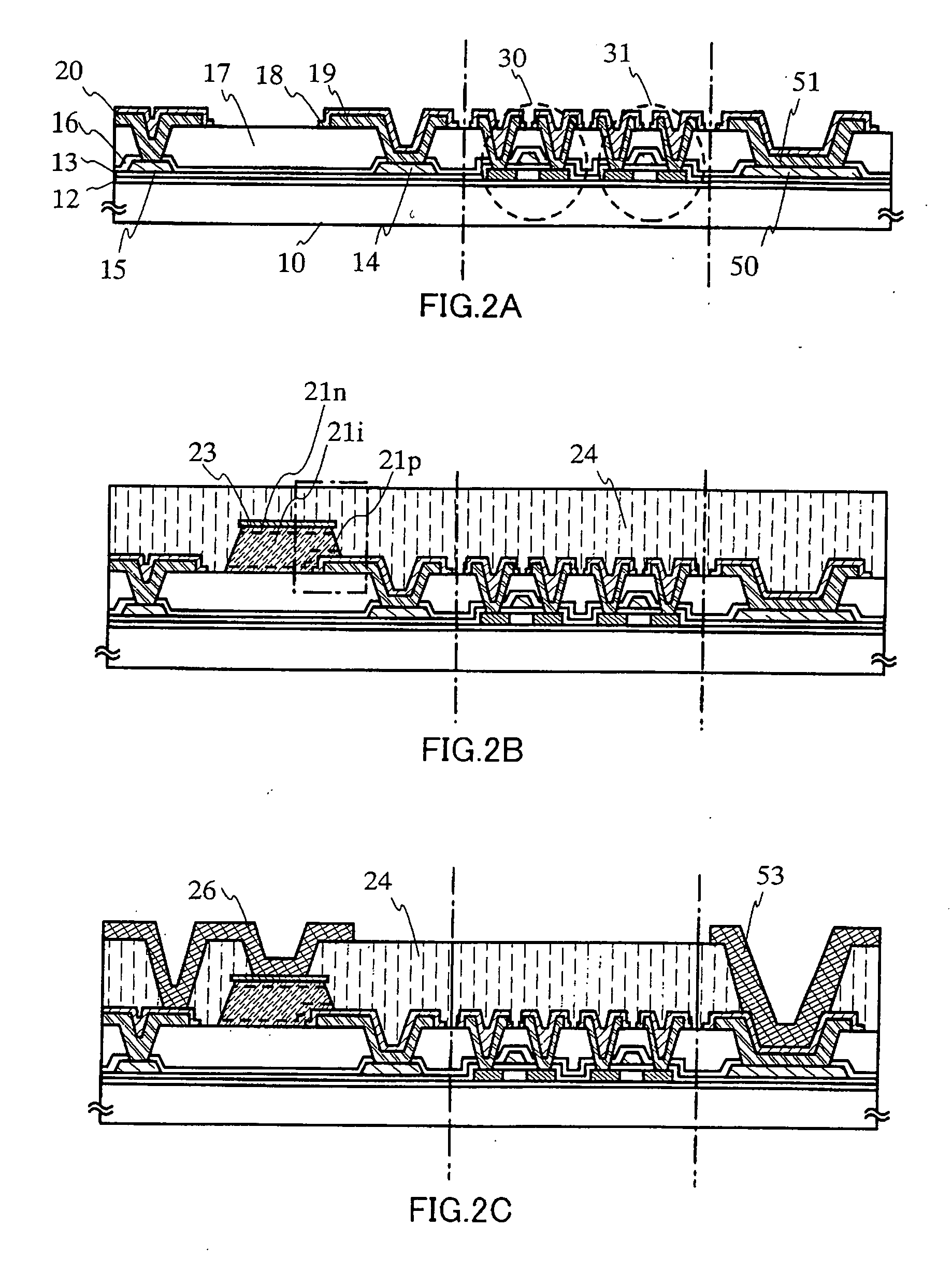
[0110] First, a TFT, a wire 19 of the TFT, and a terminal electrode 51 are formed over a glass substrate 10 similarly to Embodiment Mode 1.

[0111] Then, similarly to Embodiment Mode 1, after a conductive metal film (Ti or Mo) is formed, a resist mask is formed using a fifth photo mask and the conductive metal film is selectively etched to form a first electrode 18 which covers the wire 19. It is to be noted that a connection electrode, the terminal electrode 51, a source electrode and a drain electrode of the TFT are similarly covered with the conductive metal film.

[0112] Subsequently, similarly to Embodiment Mode 1, a p-layer (50 nm), a i-layer (600 nm), and a n-layer (70 nm) are formed to be stacked in this order using a CVD apparatus, ...

embodiment mode 3

[0123] Described in this embodiment mode is a case where a resist formation is performed by screen printing. As for the same step as that of Embodiment Mode 1 or Embodiment Mode 2, specific description thereof is omitted for simplicity.

[0124] First, a TFT, a wire 19 of the TFT, and a terminal electrode 51 are formed over a glass substrate 10 similarly to Embodiment Mode 1.

[0125] Then, similarly to Embodiment Mode 1, after a conductive metal film (Ti or Mo) is formed, a resist mask is formed using a fifth photo mask and the conductive metal film is selectively etched to form a first electrode 18 which covers the wire 19. It is to be noted that a connection electrode, the terminal electrode 51, a source electrode and a drain electrode of the TFT are similarly covered with the conductive metal film.

[0126] Subsequently, similarly to Embodiment Mode 1, a p-layer (50 nm), an i-layer (600 nm), and a n-layer (70 nm) are formed to be stacked in this order using a CVD apparatus, thereby a ...


PUM


Abstract

[Abstract]Considering further promotion of high output and miniaturization of a sensor element, it is an object of the present invention to form a plurality of elements in a limited area so that an area occupied by the element is reduced for integration. It is another object to provide a process which improves the yield of a sensor element. According to the present invention, a sensor element using an amorphous silicon film and an output amplifier circuit constituted by a thin film transistor are formed over a substrate having an insulating surface. In addition, a metal layer for protecting an exposed wire when a photoelectric conversion layer of the sensor element is patterned is provided between the photoelectric conversion layer and the wire connected to the thin film transistor.

Description

TECHNICAL FIELD [0001] The present invention relates to a semiconductor device having a sensor element and a circuit comprising a thin film transistor (hereinafter called a TFT), and a manufacturing method thereof. [0002] It is to be noted that a semiconductor device means any device which can function by utilizing semiconductor characteristics, and an electro-optical device, a semiconductor circuit, and an electronic apparatus are all included in the semiconductor device in this specification. BACKGROUND [0003] Conventionally, as a solid-state imaging element, there has been a sensor element using a single crystalline silicon substrate and a sensor element using an amorphous silicon film. [0004] A characteristic of the sensor element using a single crystalline silicon substrate is that high output is achieved by forming an output amplifier circuit over the single crystalline silicon substrate and integrating it with the sensor element. However, the form of a completed packaged unit...

Claims


Application Information

Patent Timeline
Patent Type & Authority Applications(United States)
IPC IPC(8): H01L31/0203H01L27/146H01L29/786H04N5/335H04N5/369
CPCH01L27/1214H01L27/14692H01L27/14645H01L27/14609
Inventor TAKAHASHI, HIDEKAZUMARUYAMA, JUNYAYAMADA, DAIKIKUSUMOTO, NAOTONISHI, KAZUOADACHI, HIROKISUGAWARA, YUUSUKE
Owner SEMICON ENERGY LAB CO LTD
Why Eureka
Try Eureka