Film forming apparatus, film forming method, and manufacturing method of light emitting element

a technology of film forming and light emitting elements, which is applied in the direction of vacuum evaporation coating, solid-state diffusion coating, coating, etc., can solve the problems of high power consumption of organic el elements and difficulty in applying to small or medium-sized displays, so as to reduce strain and defects, and reduce strain and defects

Inactive Publication Date: 2007-08-16
SEMICON ENERGY LAB CO LTD
View PDF11 Cites 52 Cited by
  • Summary
  • Abstract
  • Description
  • Claims
  • Application Information

AI Technical Summary

Benefits of technology

[0049]In the case of forming a film by a vapor deposition method, by providing a unit for forming a film with a substance by irradiating the substance that is evaporated with a laser beam or lamp light, dangling bonds of a vapor deposition material can be recombined; therefore, a film forming apparatus for forming a film with reduced strain and defect can be provided.
[0050]In the case of forming a film by a vapor deposition method, by providing a unit for irradiating a surface of the substrate where a film is to be formed with a laser beam or lamp light, dangling bonds of a vapor deposition material can be recombined and dangling bonds of a forming surface of a thin film can be reduced; therefore, a film forming apparatus for forming a film with reduced strain and defect can be provided.
[0051]By carrying out the present invention, a film forming apparatus which can form a film with reduced strain and defect can be obtained. Further, a film forming apparatus for forming a film with a uniform quality can be obtained.
[0052]By applying a film forming method and a film forming apparatus of the present invention to manufacture a light emitting element, a light emitting element with low driving voltage can be obtained. Further, a light emitting element with high light emission efficiency can be obtained.
[0053]By irradiating a vapor deposition film on a first electrode with a laser beam, a light emitting element having a light emitting layer with reduced strain and defect can be manufactured. Further, a light emitting element having a film with a uniform quality can be manufactured.
[0054]By using a manufacturing method of a light emitting element of the present invention, a light emitting element with low driving voltage can be obtained. Further, a light emitting element with high light emission efficiency can be obtained.

Problems solved by technology

Therefore, an inorganic EL element has high power consumption and is difficult to be applied to a small or medium sized display, such as a display in a mobile phone.

Method used


Image

  • Film forming apparatus, film forming method, and manufacturing method of light emitting element
  • Film forming apparatus, film forming method, and manufacturing method of light emitting element
  • Film forming apparatus, film forming method, and manufacturing method of light emitting element

Examples


embodiment mode 1

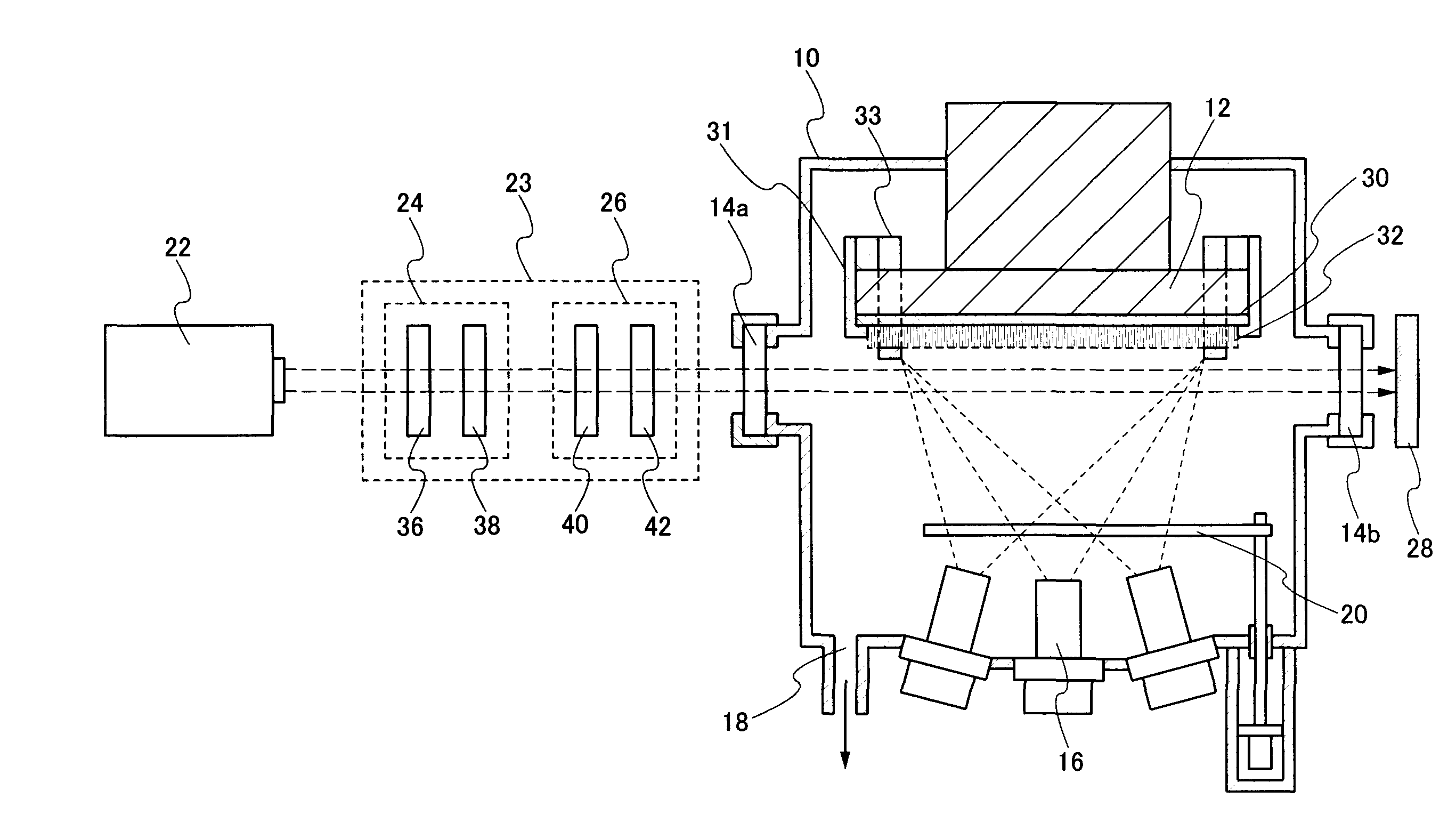
[0075]In this embodiment mode, a mode of a film forming apparatus of the present invention is described with reference to FIGS. 1 and 2. In the film forming method and the film forming apparatus described in this embodiment mode, light such as laser light is emitted in a direction parallel to a surface of a substrate or the like where a film is to be formed. FIG. 1 is a cross-sectional view illustrating a structure of the film forming apparatus and FIG. 2 is a plan view thereof. The following description is made with reference to both of the drawings.

[0076]The film forming apparatus used in this embodiment mode is structured so that a thin film which is dense and a thin film which has a uniform quality with reduced strain and defect is formed without raising a temperature to be high during film formation. Therefore, the film forming apparatus is also suitable for depositing an organic thin film which has a low evaporation temperature and a low heat-resistance temperature.

[0077]The f...

embodiment mode 2

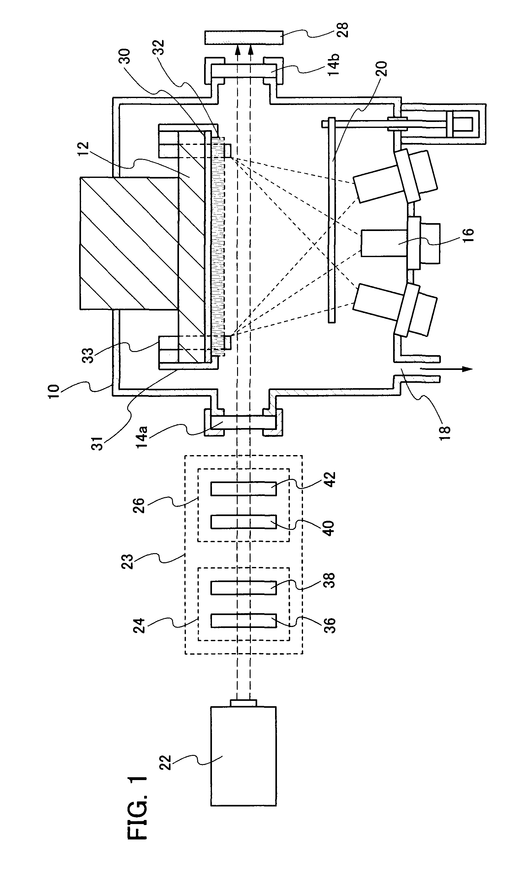
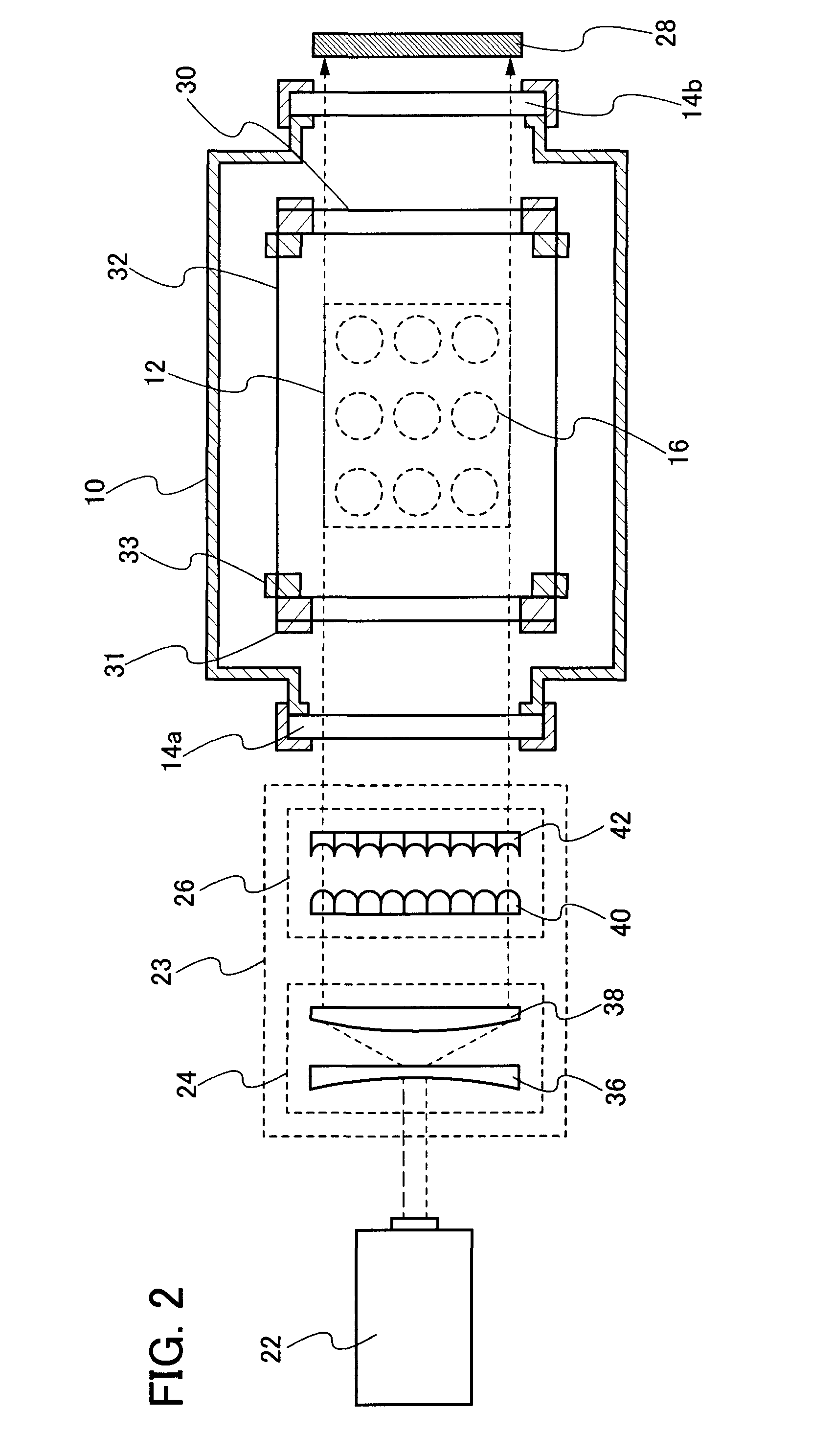
[0093]In this embodiment mode, a structure of a film forming apparatus in which a surface of a substrate where a film is to be formed can be irradiated with light such as laser light is described with reference to FIGS. 3 and 4. Note that FIG. 3 is a cross-sectional view illustrating a structure of the film forming apparatus and FIG. 4 is a plan view thereof. The description in this embodiment mode is made with reference to both of the drawings. In this embodiment mode, the same portion as that in Embodiment Mode 1 is denoted by the same reference numeral and a repeated description thereof may be omitted.

[0094]A film forming apparatus of this embodiment mode is structured so that a thin film having a favorable quality is deposited without raising a temperature to be high during film formation. Therefore, the film forming apparatus is also suitable for depositing an organic thin film which has a low evaporation temperature and a low heat-resistance temperature.

[0095]The film forming ...

embodiment mode 3

[0102]In this embodiment mode, a light emitting material used in a light emitting element of the present invention, and a forming method of the light emitting material are described. As a light emitting material used in the present invention, a material which contains a base material and at least one kind of impurity element which serves as a light emission center can be given. Note that the impurity element does not include an element which is contained in the base material.

[0103]As a base material used for a light emitting material, sulfide, oxide, or nitride can be given. As sulfide, for example, zinc sulfide (ZnS), cadmium sulfide (CdS), calcium sulfide (CaS), yttrium sulfide (Y2S3), gallium sulfide (Ga2S3), strontium sulfide (SrS), barium sulfide (BaS), or the like can be used. As oxide, for example, zinc oxide (ZnO), yttrium oxide (Y2O3), or the like can be used. As nitride, for example, aluminum nitride (AlN), gallium nitride (GaN), indium nitride (InN), or the like can be us...


PUM

PropertyMeasurementUnit
temperatureaaaaaaaaaa
outer sizeaaaaaaaaaa

Abstract

An object of the present invention is to provide a film forming method for forming a film with reduced defect and to provide a film forming method for forming a film with a uniform quality. In addition, another object is to provide a manufacturing method of a light emitting element which can be driven with low voltage. Further, another object is to provide a manufacturing method of a light emitting element with high light emission efficiency. A film with reduced defect and a uniform quality can be formed by fixing a substrate to a substrate holding unit so that at least a part of a surface of the substrate is exposed, evaporating a vapor deposition material from an evaporation source filled with the vapor deposition material, irradiating the vapor deposition material which is evaporated with a laser beam, and depositing the vapor deposition material on the surface of the substrate.

Description

BACKGROUND OF THE INVENTION[0001]1. Field of the Invention[0002]The present invention relates to a film forming method and a film forming apparatus of a thin film. In addition, the present invention relates to a manufacturing method of a light emitting element.[0003]2. Description of the Related Art[0004]Recently, display devices included in a television, a mobile phone, a digital camera, and the like are required to be flat and thin. As a display device which meets such a requirement, a display device using a self-light emitting element has drawn attention. One of self-light emitting elements is a light emitting element utilizing electroluminescence (Electro Luminescence), in which a light emitting material is interposed between a pair of electrodes, and light emission from the light emitting material can be obtained by applying voltage.[0005]Such a self-light emitting element has advantages over a liquid crystal display in that visibility of a pixel is high, backlight is not neces...

Claims


Application Information

Patent Timeline
Patent Type & Authority Applications(United States)
IPC IPC(8): B05D5/12B05D5/06C23C8/00C23C16/00
CPCB05D1/60B05D5/061H01L51/0027H01L51/001C23C14/24H10K71/164H10K71/421H05B33/10
Inventor YAMAZAKI, SHUNPEISAKATA, JUNICHIROYAMAMOTO, YOSHIAKIKATAYAMA, MIKIYOKOYAMA, KOHEIMATSUBARA, RIEKAWAKAMI, TAKAHIRO
Owner SEMICON ENERGY LAB CO LTD
Why Eureka
Try Eureka