Method and apparatus for inspecting pattern defects and mirror electron projection Type or multi-beam scanning type electron beam apparatus

a technology of electron beam apparatus and electron beam, which is applied in the direction of material analysis using wave/particle radiation, instruments, nuclear engineering, etc., to achieve the effect of quick detection of defects in semiconductor wafers

Active Publication Date: 2007-08-23
HITACHI HIGH-TECH CORP
View PDF2 Cites 31 Cited by
  • Summary
  • Abstract
  • Description
  • Claims
  • Application Information

AI Technical Summary

Benefits of technology

[0012] The present invention makes it possible to set optimum precharge conditions for a mirror electron projection type or multi-beam scanning type scanning electron beam apparatus and mirror image detection conditions, and quickly detect defects in a semiconductor wafer (specimen) in accordance with a mirror image.

Problems solved by technology

However, a condition setup technology for a mirror electron projection (MPJ) type scanning electron beam inspection technology, which emits a planar electron beam to detect mirror electrons, is not adequately considered by Japanese Patent Laid-Open No. 202217 / 2003, Japanese Patent Laid-Open No. 363085 / 2004, “Hasegawa et al., Development of EB wafer inspection technique by using mirror electron projection LSI Testing Symposium, 2004,”“Murakami et al., Development of an electron beam inspection system based on projection imaging microscopy, LSI Testing Symposium, pp.

Method used


Image

  • Method and apparatus for inspecting pattern defects and mirror electron projection Type or multi-beam scanning type electron beam apparatus
  • Method and apparatus for inspecting pattern defects and mirror electron projection Type or multi-beam scanning type electron beam apparatus
  • Method and apparatus for inspecting pattern defects and mirror electron projection Type or multi-beam scanning type electron beam apparatus

Examples


first embodiment

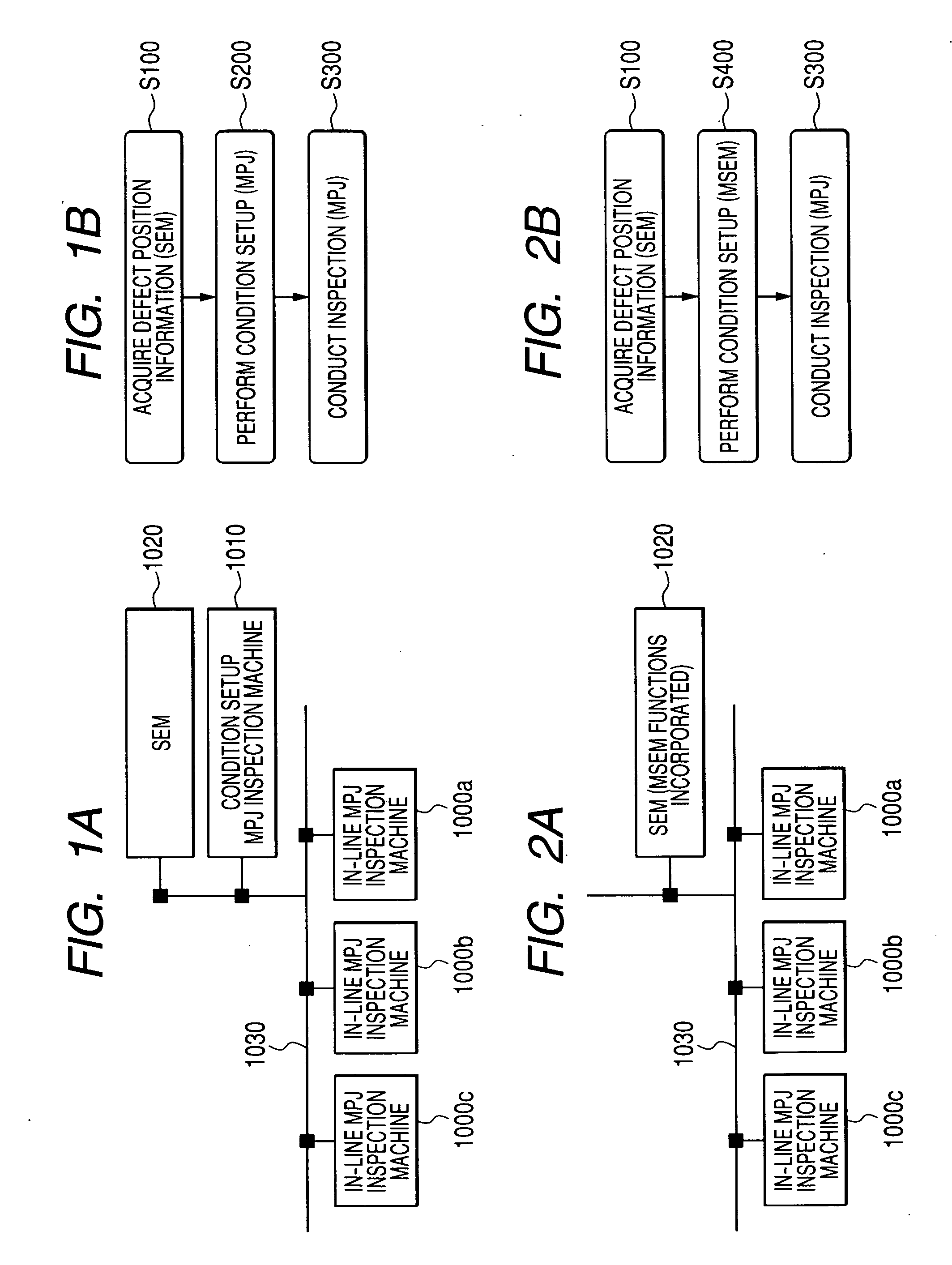
[0033] A first embodiment of a method and system configuration for mirror electron projection type or multi-beam scanning type scanning electron beam pattern defect inspection including condition setup will now be described with reference to FIGS. 1A and 1B.

[0034] As shown in FIG. 1A, the first embodiment includes an SEM 102, which acquires defect position information; a mirror electron projection (MPJ) type (secondary electron projection (SEPJ) type included) or multi-beam scanning type inspection machine for condition setup 1010, which performs condition setup; a plurality of mirror electron projection type (MPG type (SEPJ type included) or multi-beam scanning type in-line inspection machines 1000a-1000c; and a network 1030, which interconnects the above devices. The plurality of in-line inspection machines 1000a-1000c are installed by incorporating them into a semiconductor manufacture line. As the mirror electron projection type or multi-beam scanning type inspection machine fo...

second embodiment

[0035] A second embodiment of a method and system configuration for mirror electron projection type or multi-beam scanning type scanning electron beam pattern defect inspection including condition setup will now be described with reference to FIGS. 2A and 2B.

[0036] As shown in FIG. 2A, the second embodiment includes an SEM 1020, which doubles as an MSEM (The MSEM in the SEM is configured to adjust the electrical potential of an electrode on the specimen so that incident beam electrons' kinetic energy prevailing directly above the specimen is approximately zero.) to acquire defect position information and perform condition setup; a plurality of mirror electron projection type (MPJ type (SEPJ type included) or multi-beam scanning type in-line inspection machines 1000a-1000c; and a network 1030, which interconnects the above devices. The plurality of mirror electron projection type or multi-beam scanning type in-line inspection machines 1000a-1000c are installed by incorporating them ...

first example

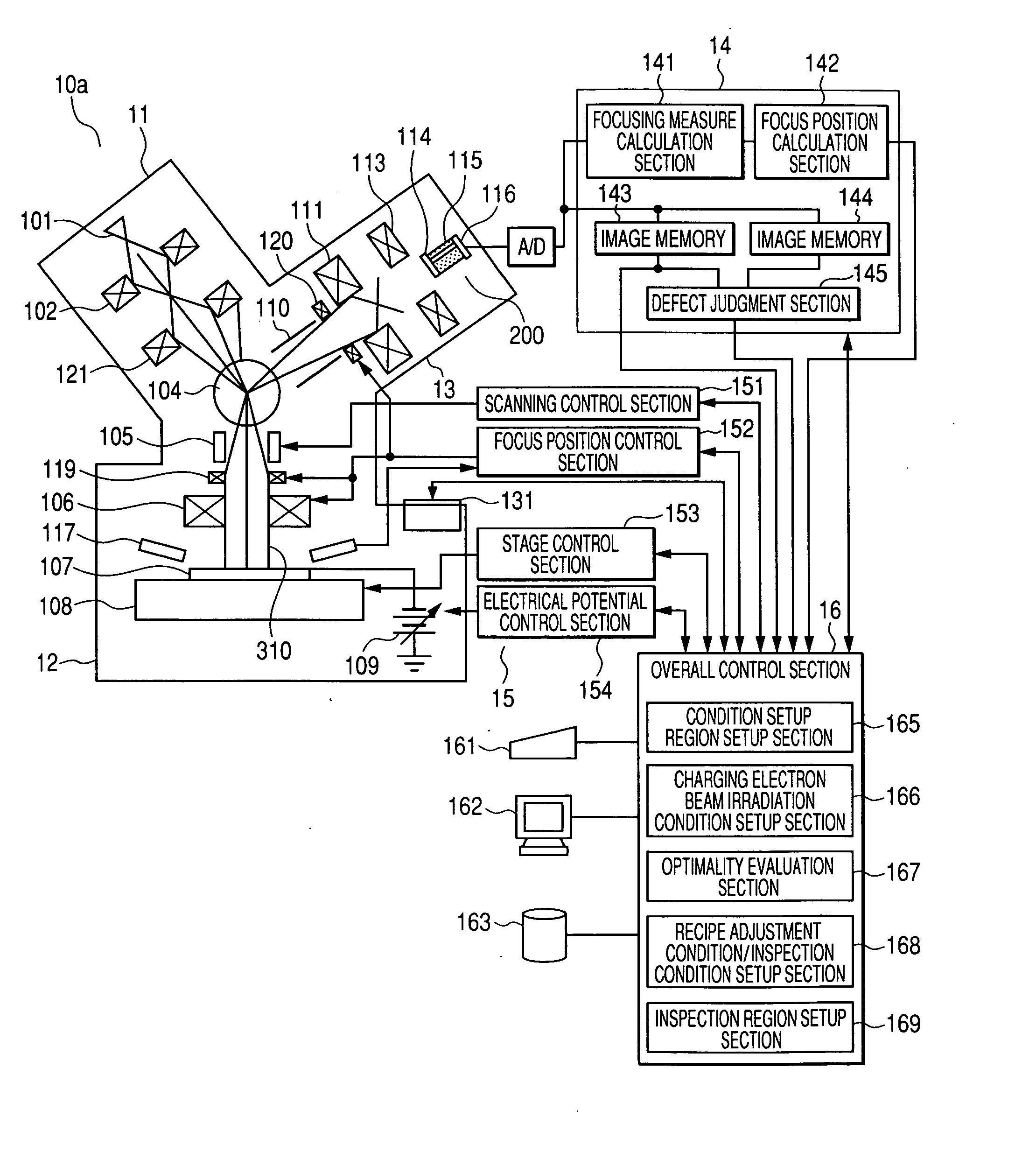
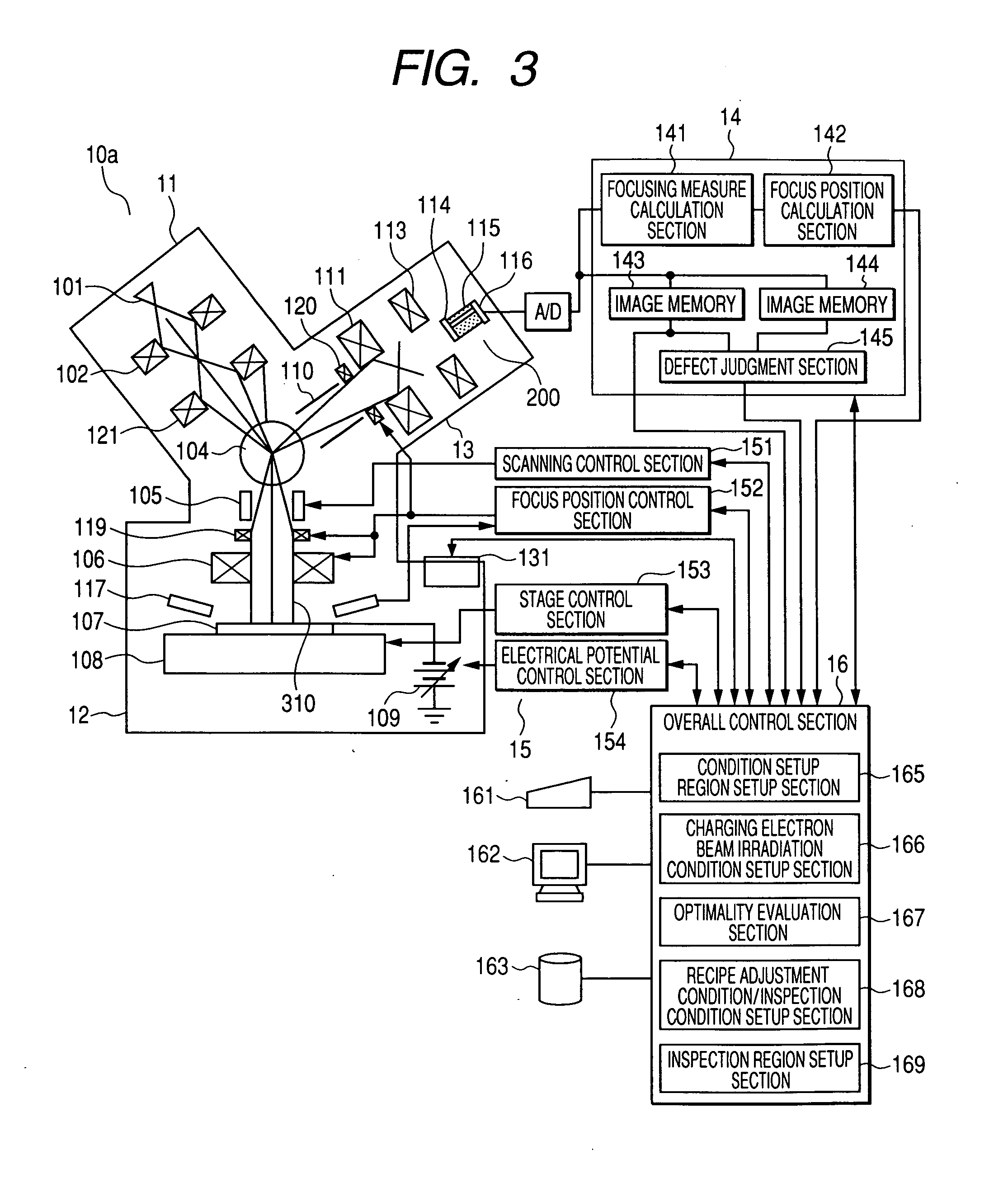
[0037] A mirror electron projection type (MPJ type (SEPJ type included) inspection machine (scanning electron beam apparatus) 10a, which is the first example of scanning electron beam apparatuses (inspection machines) 1000, 1010 for use in defect inspection and condition setup according to the present invention will now be described with reference to FIGS. 3, 4A, and 4B. The MPJ type scanning electron beam apparatus uses a method of mirror electron detection based on mirror electron projection, which emits a planar electron beam. The SEPJ type scanning electron beam apparatus uses a method of secondary electron detection based on mirror electron projection, which emits a planar electron beam. FIG. 3 shows a configuration of the first example of a scanning electron beam apparatus according to the present invention. Roughly speaking, the first example includes an electron irradiation optics 11, a specimen chamber 12, an electron image formation optics 13, an image processing section 1...


PUM


Abstract

The present invention provides a mirror electron projection (MPJ) type (SEPJ type included) scanning electron beam apparatus that is capable of performing condition setup, and a method and apparatus for inspecting pattern defects with the scanning electron beam apparatus. A mirror electron projection type defect inspection apparatus, which comprises a charging device for emitting a charging electron beam, electron beam irradiation means for shedding a mirror electron projection electron beam onto an inspection region near which an electrical potential distribution is formed, detection means for detecting secondary electrons or reflected electrons generated from a surface and proximity of the specimen, and defect detection means for detecting a defect by processing a mirror image signal that is detected by the detection means, includes irradiation condition optimization means for optimizing charging electron beam irradiation conditions.

Description

BACKGROUND OF THE INVENTION [0001] The present invention relates to a mirror electron projection (MPJ) type (secondary electron projection (SEPJ) type included) or multi-beam scanning type electron beam apparatus, which irradiates an inspection target with a planar electron beam to detect mirror electrons, and to a method and apparatus for inspecting pattern defects with the electron beam apparatus. [0002] A mirror electron projection type semiconductor wafer scanning electron beam apparatus, which emits a planar electron beam for throughput enhancement, is disclosed, as a replacement for a scanning type that emits a point electron beam, by Japanese Patent Laid-Open No. 202217 / 2003, “Hasegawa et al., Development of EB wafer inspection technique by using mirror electron projection, LSI Testing Symposium, 2004,”“Murakami et al., Development of an electron beam inspection system based on projection imaging microscopy, LSI Testing Symposium, pp. 85-87, 2004,”“Nagahama et al., Inspection...

Claims


Application Information

Patent Timeline
Patent Type & Authority Applications(United States)
IPC IPC(8): G21K7/00
CPCH01J37/026H01J2237/2817H01J2237/0048H01J37/292
Inventor OKUDA, HIROHITOHIROI, TAKASHIHASEGAWA, MASAKITANAKA, SHIGEYA
Owner HITACHI HIGH-TECH CORP
Why Eureka
Try Eureka