Nanostructured electroluminescent device and display

a technology of electroluminescent devices and nanostructures, applied in the direction of discharge tube luminescnet screens, natural mineral layered products, transportation and packaging, etc., can solve the problems of short life of oleds, loss of color balance, and several material-based and manufacturing process-dependent problems, so as to improve efficiency and reduce display life , the effect of improving efficiency

Inactive Publication Date: 2007-08-23
FIRST SOLAR INC (US)
View PDF55 Cites 63 Cited by
  • Summary
  • Abstract
  • Description
  • Claims
  • Application Information

AI Technical Summary

Benefits of technology

[0007] Display devices made with QDs have quantum efficiencies which are an order of magnitude lower than OLED. QDs have been combined with OLED materials to improve efficien

Problems solved by technology

OLED displays suffer from several materials based and manufacturing process dependant problems.
For example, OLEDs have short lifetimes, loss of color balance over time, and a high cost of manufacturing.
The poor lifetime and color balance issues are due to the chemical properties of emissive device in the OLED.
For example, it is difficult to improve the lifetime of blue OLEDs because the higher energy in the blue spectrum tends to destabilize the organic molecules used in the OLED.
The

Method used


Image

  • Nanostructured electroluminescent device and display
  • Nanostructured electroluminescent device and display
  • Nanostructured electroluminescent device and display

Examples


example 1

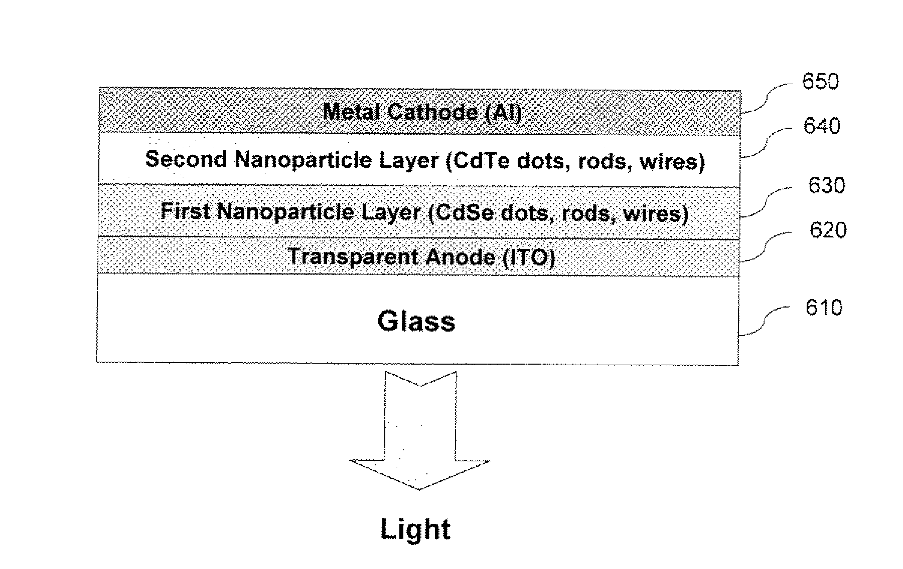
[0041] A nanostructured electroluminescent device is shown in FIG. 6, a transparent conducting layer ITO 620 is deposited on glass substrate (610) by following methods well known in the art. The surface of the ITO can be exposed to plasma treatment or other processes well known in the art to adjust the work function of ITO. A first charge conducting nanoparticle layer (630) is then deposited on the ITO layer. Spin coating or ink-jet printing or other printing process can be used to deposit nanoparticles dispersed in a suitable solvent. A continuous pin hole free nanoparticle layer can be obtained by heating the substrate to about 200 C for about 15 minutes to drive off the solvent. The nanoparticles in layer 630 can be dots, rods or wires. The first nanoparticle layer in this embodiment is made from CdSe. Second nanoparticle layer (640) is deposited directly on top of the first nanoparticle layer (630). Spin coating or ink-jet printing or other printing process can be used to deposi...

example 2

[0042] Another embodiment of a nanostructured electroluminescent device is shown in FIG. 7. A transparent conducting layer ITO (720) is deposited on glass substrate (710). As described in Example 1, a hole injection layer (730) such as aluminum oxide is deposited on lTO layer 720 by the methods known in the art. The first and second nanoparticle layers (740 and 750), are then deposited as described in Example 1. An electron injecting layer (760) such as LiF is then deposited on top of the second nanoparticle layer by methods well known in the art. An Aluminum metal electrode (670) is deposited on top of the second nanoparticle layer to complete the nanostructured electroluminescent device.

example 3

[0043] Another embodiment of a nanostructured electroluminescent display shown in FIG. 8. The ITO hole injection and first and second nanoparticle layers are formed as described in Example 2. A hole blocking layer made of TiO2 (860) is deposited on top of the second nanoparticle layer by the methods well known in the art. An electron injecting layer (870) such as LiF is then deposited by methods well known in the art and an Aluminum metal electrode (80) is deposited on top of the second nanoparticle layer to complete the nanostructured electroluminescent device.


PUM

PropertyMeasurementUnit
Thicknessaaaaaaaaaa
Electrical conductoraaaaaaaaaa
Electric potential / voltageaaaaaaaaaa

Abstract

An electroluminescent device contains (1) first and second electrodes, at least one of which is transparent to radiation; (2) a hole conducting layer containing first nanoparticles wherein the hole conducting layer is in contact with said first electrode; (3) an electron conducting layer containing second nanoparticles where the electron conducting layer is in contact with the hole conducting layer and the second electrode; and optionally (4) a voltage source capable of providing positive and negative voltage, where the positive pole of the voltage source is connected to the first electrode and the negative pole is connected to the second electrode. In some embodiments, the electroluminescent device also includes an electron-hole combination layer between the hole and electron conducting layers.

Description

CLAIM OF PRIORITY [0001] This application claims the benefit of U.S. Provisional Application Ser. No. 60 / 774,794, filed Feb. 17, 2006, under 35 U.S.C. §119(e) and is incorporated herein by reference in its entirety.FIELD OF THE INVENTION [0002] The invention relates to electroluminescent devises and emissive displays containing them. BACKGROUND OF THE INVENTION [0003] Emissive displays fall under three categories depending on the type of emissive device in the display: (1) Organic Light Emitting Displays (OLED), (2) Field Emission Displays (FED) and (3) Inorganic Thin Film Electroluminescent Displays (EL). Of these three categories, OLEDs have received the most attention and investment around the world. Approximately 100 companies are developing various aspects of the OLED technology. Commercial OLED products are in the mobile phone and MP3 markets. OLED devices can be made from small molecules (pioneered by Kodak) or polymers (pioneered by Cambridge Display Technology). OLED device...

Claims


Application Information

Patent Timeline
IPC IPC(8): H05B33/12H01L31/00
CPCB82Y20/00B82Y30/00C09K11/883Y10T428/25H01L51/5048H01L51/5088H05B33/14H01L51/5012H10K50/115H10K50/14H10K50/17H10K50/11H10K2102/331H01L21/02576H01L21/02579H10K50/171
Inventor REDDY, DAMODER
Owner FIRST SOLAR INC (US)
Why Eureka
Try Eureka