Semiconductor laser diode and integrated semiconductor optical waveguide device

Active Publication Date: 2007-08-23
LUMENTUM JAPAN INC
View PDF2 Cites 17 Cited by
  • Summary
  • Abstract
  • Description
  • Claims
  • Application Information

AI Technical Summary

Benefits of technology

[0017] According to the present invention, a semiconductor laser diode having a high output power and a low threshold current can be realized. At the same time, in an integrated semiconductor optical waveguide device such as EA/DFB, the semiconductor laser diode and the electroabsorption type optical modulator can not only be

Problems solved by technology

Although this may be met by increasing an operating current, it is disadvantageous for reduction in power consumption.
However, power consumption increases with an increase in transmission distance as well as with the use of higher bit rate.
Since the amount of heat generated becomes larger in general as the operating current in a semiconductor laser diode is raised, optical power is saturated at a certain current level, thereby making it impossible to obtain enough output.
However, no semiconductor optical waveguide device integrated with a high power laser in which ridge is widened or threshold current is lowered as described above has been disclosed.
As described above, the insertion of the upper buffer layer between the upper clad layer and the ridge is effective for power enhancement of a semiconductor laser diode, whereas there has been a problem that lateral diffusion of carrier becomes larger particularly on the p-side and the threshold current is increased.
This causes an increase in loss of coupling to an exterior such as fiber.
However, this method requires crystal regrowth to form a cover layer.
Therefore, it is disadvantageous in terms of cost reduction, and further, the application of the method is limited to InP-substrate bas

Method used


Image

  • Semiconductor laser diode and integrated semiconductor optical waveguide device
  • Semiconductor laser diode and integrated semiconductor optical waveguide device
  • Semiconductor laser diode and integrated semiconductor optical waveguide device

Examples


Example

Embodiment 1

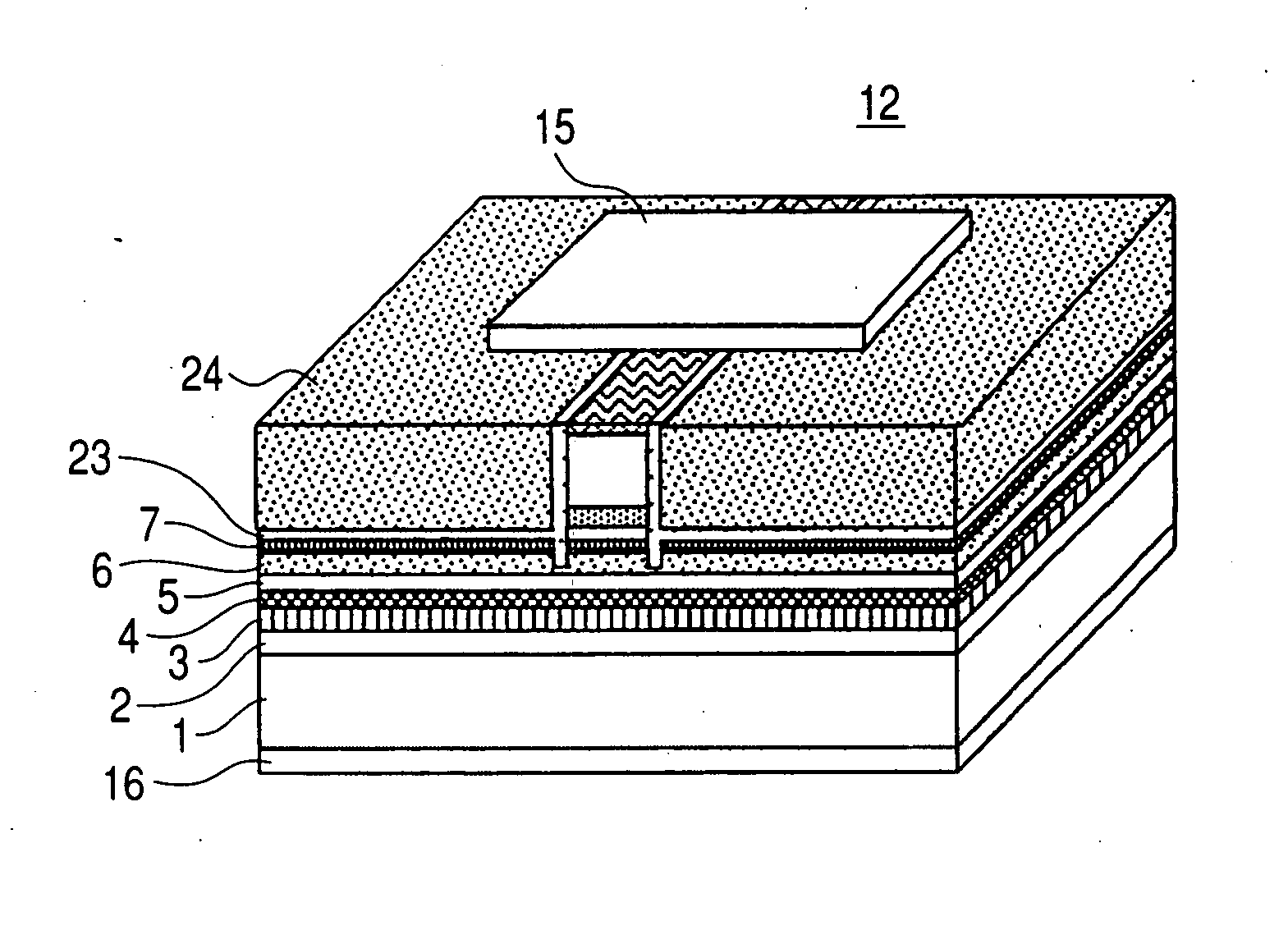
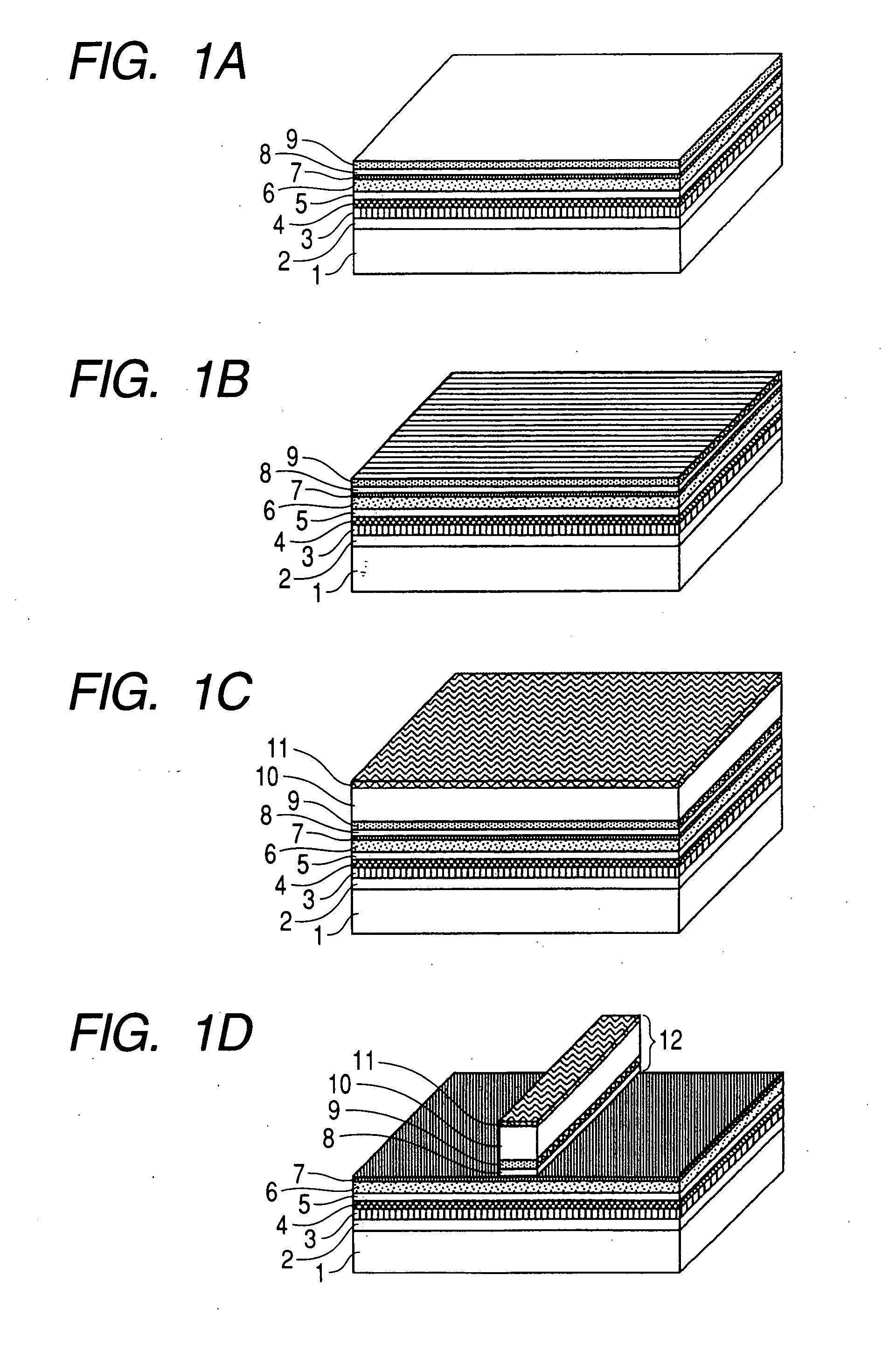
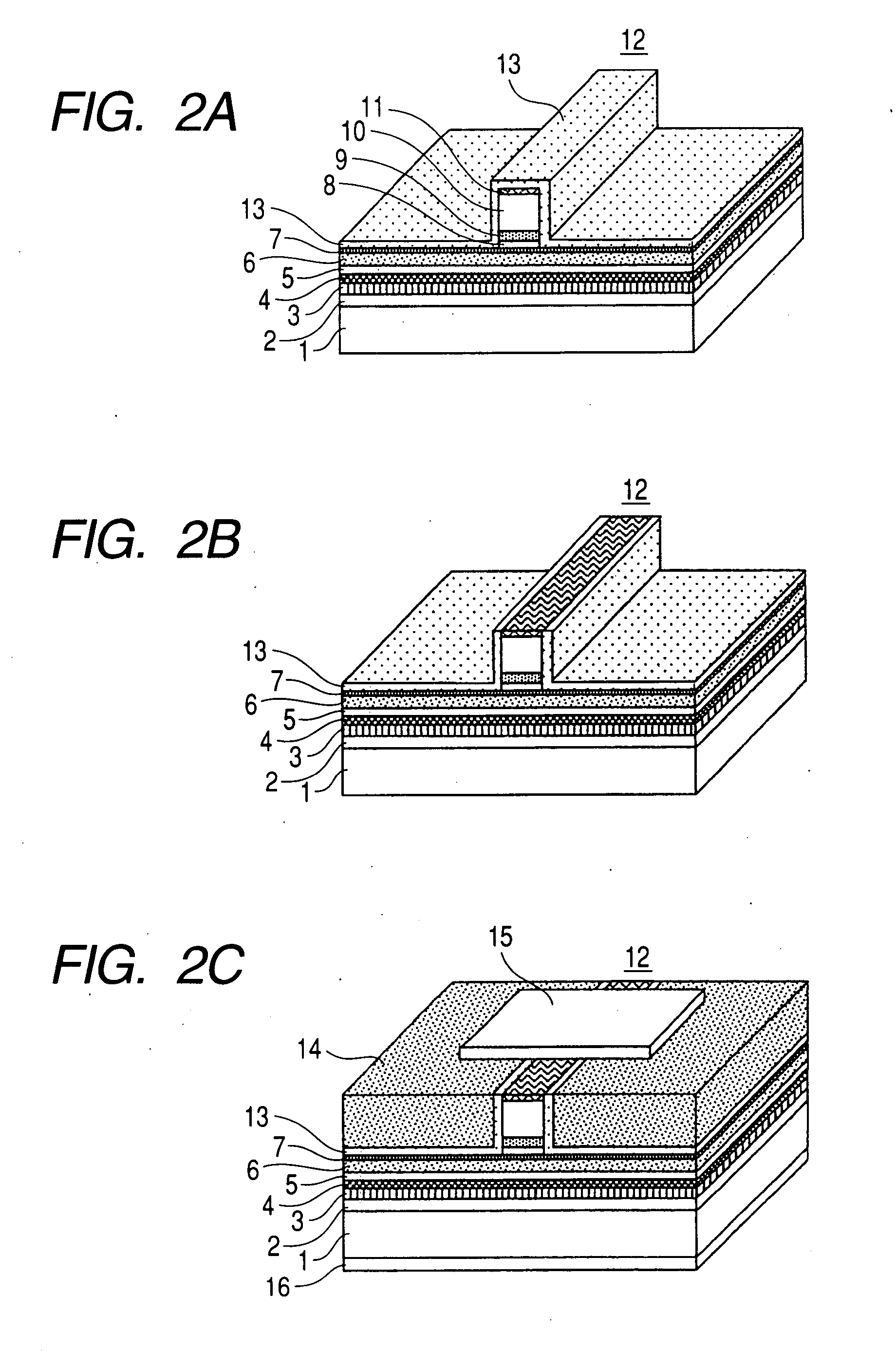
[0033] Embodiment 1 in which the present invention was applied to a 1.5 μm-wavelength band ridge waveguide type semiconductor laser diode is explained first. It should be noted that the figure size and the scale described in Embodiment 1 do not necessarily correspond proportionately. A semiconductor laser diode having an upper buffer layer as the premise of the present invention is explained using FIGS. 1 and 2, and then an embodiment of a semiconductor laser diode of the present invention in which insulative grooves with a low refractive index that were cut into the upper buffer layer along both sides of the ridge were formed is explained.

[0034] As shown in FIG. 1A, on an n-type InP semiconductor substrate 1 (thickness 2 mm), an n-type InP buffer layer 2 (thickness 0.15 μm), a lower clad layer 3 (thickness 0.13 μm) formed of n-type InGaAsP series, a multiple-quantum well active layer 4 (thickness 0.114 μm) in which a well layer formed of InGaAsP (thickness 7 nm, compo...

Example

Embodiment 2

[0061] A semiconductor laser diode applied with the present invention can also be realized by a structure starting with an n-type GaAs semiconductor substrate in place of the structure starting with the n-type InP semiconductor substrate. FIGS. 8A to 8C are diagrams showing as Embodiment 2 the semiconductor laser diode realized by the structure starting with the n-type GaAs semiconductor substrate.

[0062] The semiconductor laser diode shown in Embodiment 2 is different in materials and part of the manufacturing process because the starting substrate is different but can be constructed by steps similar to those in Embodiment 1, and therefore explained in a simplified manner.

[0063] As shown in FIG. 8A, on an n-type GaAs semiconductor substrate 31 (thickness 2 mm), an n-type GaAs buffer layer 32 (film thickness 0.5 μm), a lower clad layer 33 (film thickness 2.5 μm) formed of n-type (AlxGa1-x)0.5In0.5P (x=0.60), a multiple-quantum well active layer 34 (thickness 0.024 μm) ...

Example

Embodiment 3

[0069] An example of the integrated semiconductor optical waveguide device to which the present invention was applied is explained in Embodiment 3 with reference to FIGS. 9A to 9E, FIGS. 10A to 10E, and FIG. 11. It should be noted that the figure is used strictly for the purpose of explaining the present embodiment and the figure size and the scale described in the present embodiment do not necessarily correspond proportionately.

[0070] As shown in FIG. 9A, on an n-type InP semiconductor substrate 51 (thickness 2 mm), an n-type InP buffer layer 52 (film thickness 0.5 μm), a lower clad layer of electroabsorption type optical modulator 53 (film thickness 0.1 μm) formed of n-type InGaAlAs (compositional wavelength 0.92 μm), a multiple-quantum well active layer 54 in which a well layer (film thickness 7 nm, compositional wavelength 1.5 μm) formed of InGaAlAs having 0.6% compressive strain and a barrier layer (film thickness 10 nm, compositional wavelength 1.35 μm) formed of...


PUM


Abstract

A conventional semiconductor laser diode is small in optical power at a constant operating current and limited in ridge width when integrated with an optical device, which forces the integration to be performed by lowering the original characteristic and makes it difficult to reduce cost and power consumption. In a semiconductor laser diode, widening of the ridge width is made possible by lowering the difference in refractive indexes between the ridge and other components, diffusion current and increase in the difference of refractive indexes are prevented by forming approximately vertical grooves along both sides of the ridge, and deterioration in characteristics due to regrowth is prevented by forming a diffraction grating on the ridge. The semiconductor laser diode is integrated with an optical device such as electroabsorption type optical modulator without increase of growth cycles and without restriction of the ridge width by using a tapered waveguide.

Description

[0001] The present application claims priority from Japanese application JP 2006-044887 filed on Feb. 22, 2006, the content of which is hereby incorporated by reference into this application. FIELD OF THE INVENTION [0002] The present invention relates to a semiconductor laser diode and an integrated optical waveguide device in which the semiconductor laser diode and an optical modulator are integrated. BACKGROUND OF THE INVENTION [0003] Recently, it is becoming increasingly important to reduce power consumption and cost of a semiconductor laser diode and an integrated semiconductor optical waveguide device in which a semiconductor laser diode and an electroabsorption type optical modulator are integrated. For the semiconductor laser diode, there are mainly ridge type and buried heterostructure type, of which the ridge type is advantageous for cost reduction because of its easier fabrication and smaller number of growth steps and is actively developed for use in both information and ...

Claims


Application Information

Patent Timeline
IPC IPC(8): H01S5/00H01S3/04H01S5/12
CPCB82Y20/00H01S5/0265H01S5/1014H01S5/12H01S5/2004H01S5/22H01S2301/173H01S5/2214H01S5/2216H01S5/3211H01S5/3406H01S5/3434H01S5/2213
Inventor FUKAMACHI, TOSHIHIKOMAKINO, SHIGEKITANIGUCHI, TAKAFUMIAOKI, MASAHIRO
Owner LUMENTUM JAPAN INC
Why Eureka
Try Eureka