Semiconductor integrated circuit apparatus and method of designing the same

Inactive Publication Date: 2007-08-30
PANASONIC CORP
View PDF7 Cites 6 Cited by
  • Summary
  • Abstract
  • Description
  • Claims
  • Application Information

AI Technical Summary

Benefits of technology

[0007]In consideration of the actual circumstances, the invention has been made and has an object to provide a semiconductor integrated circuit apparatus capable of enhancing precision in a pattern, reducing a variation in a wiring capacity and improving a degree of freedom of a wiring.
[0008]Moreover, it is an object of the invention to provide a semiconductor integrated circuit apparatus capable of giving a power wiring which is wide and has no possibility of a short circuit without reducing a degree of freedom of a wiring in a core cell on a chip surface.
[0010]By the structure, it is possible to regulate an area of a power wiring cell by forming the slit. It is possible to prevent a variation in etching or a wiring capacity from being caused in a formation of a pattern. More specifically, it is possible to eliminate a problem of a short circuit due to a slight positional shift caused by an increase in a width of the wiring. Thus, it is possible to cause a pattern on a chip surface to be uniform in the formation of the pattern, and furthermore, to reduce the variation in the wiring capacity. Thus, it is possible to provide a desirable power wiring without reducing a degree of freedom of the wiring in a core cell.
[0012]By the structure, it is possible to provide a power wiring having no possibility of a shirt circuit which might be caused by an increase in a width without reducing a degree of freedom of the wiring in the core cell.
[0029]According to the structure, it is possible to avoid a short circuit with the wiring in the core cell at the step of processing a wide metal which is caused in the case in which the height of the power wiring cell is increased and to maintain a wiring track between the cells without reducing a degree of freedom of the metal wiring in the core cell.
[0030]Moreover, the power wiring cell has the shape. Consequently, an area ratio of the metal wiring can be maintained and a pattern on a chip surface can be caused to be uniform.

Problems solved by technology

For this reason, it is hard to give access to an input / output terminal in a reduced cell and there is thus increased a possibility that a local wiring jam might be generated in each place.
However, this reduces the degree of freedom of the wiring in the core cell.
In some cases, therefore, an area ratio of the power wiring causes a problem of a variation in the wiring capacity in addition to the generation of a uniform pattern on a chip surface in the formation of the pattern.

Method used


Image

  • Semiconductor integrated circuit apparatus and method of designing the same
  • Semiconductor integrated circuit apparatus and method of designing the same
  • Semiconductor integrated circuit apparatus and method of designing the same

Examples


first embodiment

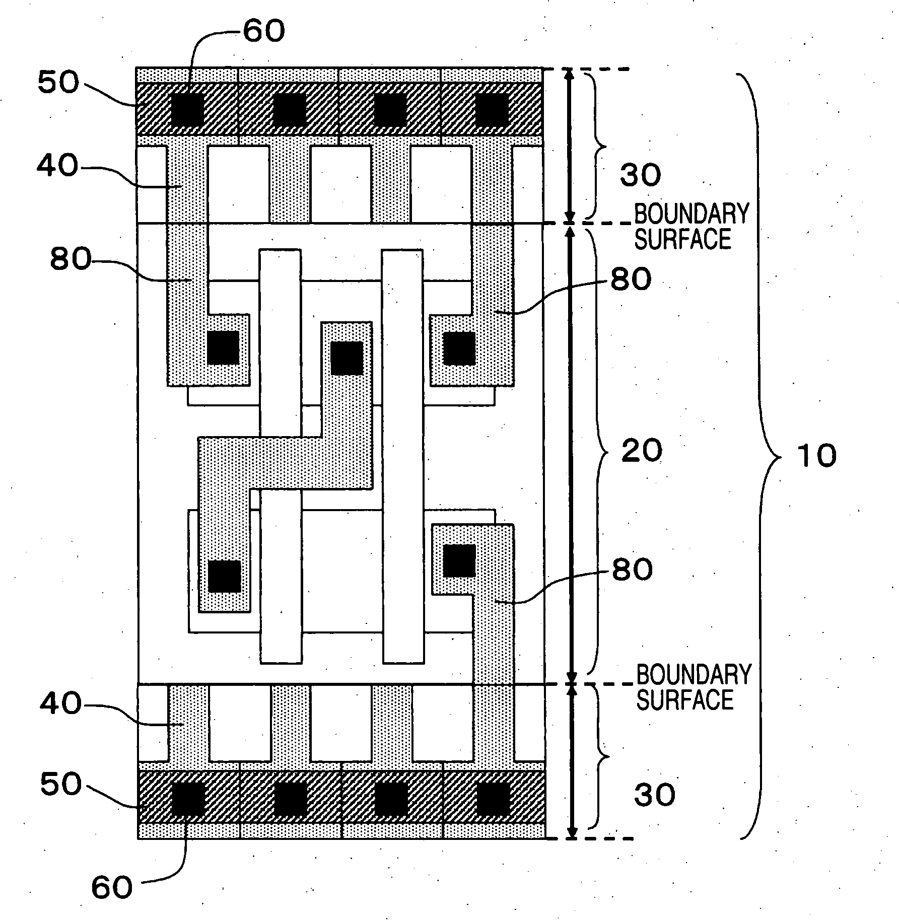
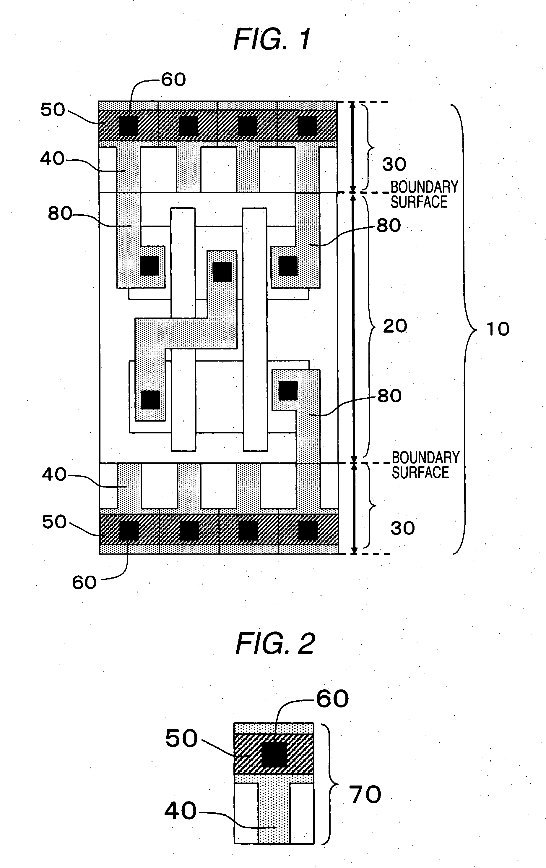
[0044]FIG. 1 shows an example of a structure of a semiconductor integrated circuit apparatus according to a first embodiment of the invention.

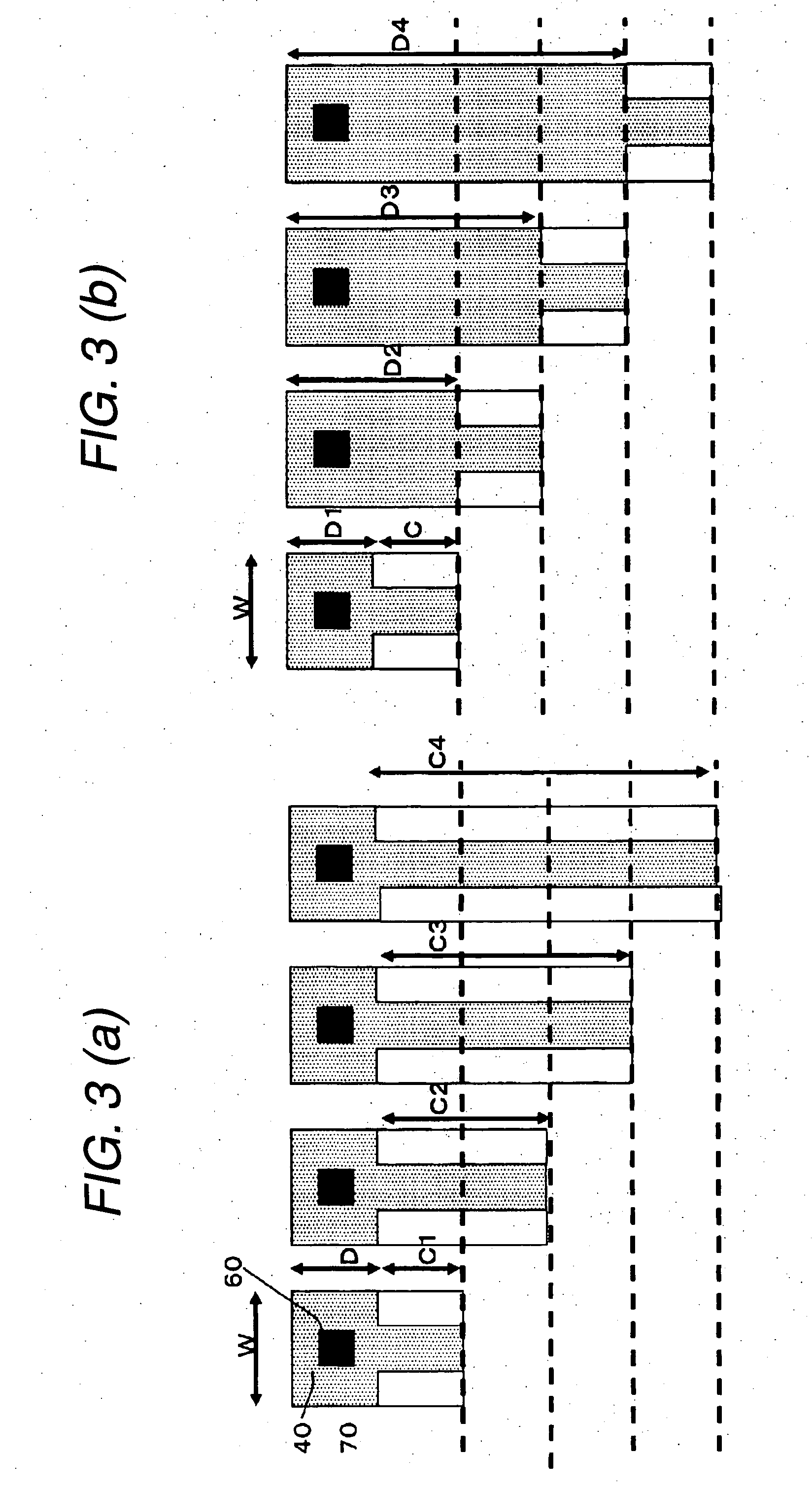
[0045]A logic cell 10 in FIG. 1 is formed by a core cell 20 constituting a circuit function (for example, an inverter, an AND, an NAND, an NOR, a latch and a flip-flop) and a power wiring cell 30 including a power wiring. The power wiring cell 30 is disposed on both sides of the core cell 20 without respective boundaries overlapping each other, and one of them supplies a source voltage and the other supplies a ground voltage. As shown in FIG. 2, the power wiring cell 30 is constituted by a power wiring unit cell 70 having a metal wiring 40, an active region 50 for holding an electric potential of a substrate to be constant, and a contact 60 for electrically connecting the metal wiring 40 to the active region 50. The metal wiring 40 takes a shape of T and the power wiring unit 70 is disposed adjacently on left and right so that a power wiring e...

second embodiment

[0052]FIGS. 4 and 5 show an example of a structure of a semiconductor integrated circuit apparatus according to a second embodiment of the invention.

[0053]FIG. 4 shows a power wiring unit cell 700 constituted by only an active region 500 for holding an electric potential of a substrate to be constant.

[0054]Although the metal wiring 40 of the power wiring unit cell 70 takes the shape of T in the first embodiment, it is possible to form a power wiring extended in a direction of a cell train in a chip in the same manner as in the power wiring unit cell 70 by forming the T shape in the active region 500 and disposing the T shape adjacently on left and right in the power wiring unit cell 700 according to the embodiment.

[0055]In the case in which a metal wiring 80 in the core cell is formed by the active region, it is connected to a wiring extended in a perpendicular direction of the T-shaped active region of the power wiring unit cell 700 so that a power can be supplied into the core cel...

third embodiment

[0058]FIG. 6 shows an example of a structure of a semiconductor integrated circuit apparatus according to a third embodiment of the invention.

[0059]A logic cell 11 shown in FIG. 6 is constituted by a core cell 21 and a power wiring cell 31. The power wiring cell 31 is disposed on upper and lower parts of the core cell 21 without respective boundaries overlapping each other, and one of the power wiring cells 31 supplies a source voltage and the other supplies a ground voltage. As shown in FIG. 7, moreover, the power wiring cell 31 is constituted by a power wiring unit cell 71 having a metal wiring 41, an active region 51 for holding an electric potential of a substrate to be constant, and a contact 60 for electrically connecting the metal wiring 41 to the active region 51. By disposing the power wiring unit cell 71 adjacently on left and right, it is possible to form a power wiring extended in a direction of a cell train in a chip.

[0060]Although the power wiring unit cell 70 takes th...


PUM


Abstract

In a semiconductor integrated circuit apparatus formed by a core cell constituting a circuit function and a power wiring cell including a power wiring, a metal of a power wiring unit cell constituting the power wiring cell is formed to take a shape of T, and the power wiring unit cell is disposed adjacently, thereby forming a serial power wiring. The core cell and the power wiring cell are connected to each other through a metal wiring in the core cell in which coordinates in a horizontal direction are preset, and a power signal is thus supplied.

Description

BACKGROUND OF THE INVENTION[0001]1. Field of the Invention[0002]The present invention relates to a semiconductor integrated circuit apparatus and a method of designing the same, and more particularly to a power wiring structure in a logic cell and a designing method.[0003]2. Description of the Related Art[0004]In recent years, referring to a semiconductor device to be loaded into a semiconductor integrated circuit apparatus, a demand for a reduction in an area of a standard logic cell has been increased more and more with a microfabrication, while the number of gates to be mounted on one chip has been increased in order to implement a device having more multifunctions. For this reason, it is hard to give access to an input / output terminal in a reduced cell and there is thus increased a possibility that a local wiring jam might be generated in each place. As a countermeasure to be taken against the problem, layout means has been disclosed in JP-A-2003-167934. FIG. 12(a) shows an exam...

Claims


Application Information

Patent Timeline
IPC IPC(8): H01L23/48
CPCH01L27/118H01L27/0207
Inventor IKEGAMI, TOMOAKINISHIMURA, HIDETOSHI
Owner PANASONIC CORP
Why Eureka
Try Eureka