
Low power memory architecture

a memory architecture and low power technology, applied in the field of memory, can solve the problems of more complicated bitline sense amplifier control circuitry, unacceptably long time required to activate the device from the off state, and unacceptably long time required to activate the device, so as to minimize current leakage, minimize current leakage, and reduce the effect of leakage curren

Active Publication Date: 2007-08-30
CONVERSANT INTPROP MANAGEMENT INC
View PDF12 Cites 29 Cited by
  • Summary
  • Abstract
  • Description
  • Claims
  • Application Information

AI Technical Summary

Benefits of technology

[0016] It is an object of the present invention to provide a memory architecture and circuits for minimizing current leakage in the memory array. In particular, it is an object of the invention to minimize current leakage by disconnecting the power supplies from a memory array hierarchically organized into blocks during a low power mode of operation, and then connecting the power supplies only to the block of the memory array to be accessed. Leakage current can be further reduced by a databus precharge scheme in which databuses are precharged to one voltage during idle times and a second voltage during active read cycles, such that leakage current in datapath circuitry connected to the databuses within the memory array blocks is reduced.

Problems solved by technology

While users can turn off the device to truly maximize power conservation, the time required to activate the device from the off state is unacceptably long.
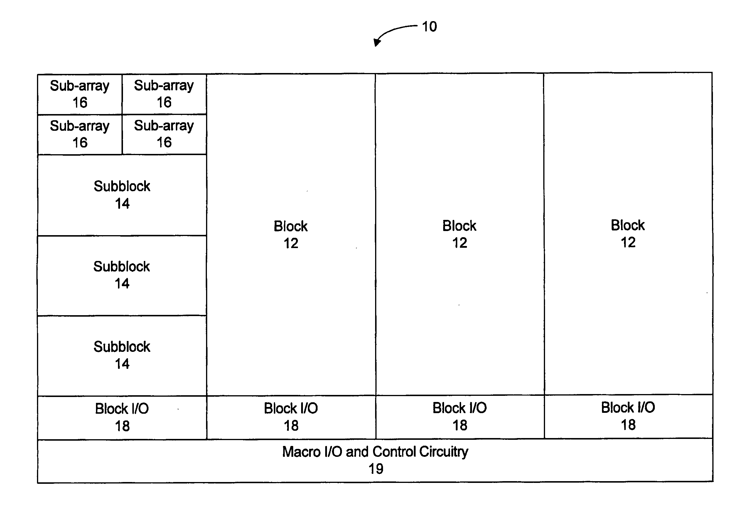
Current leakage is also a problem during an active operating mode of the memory 10.
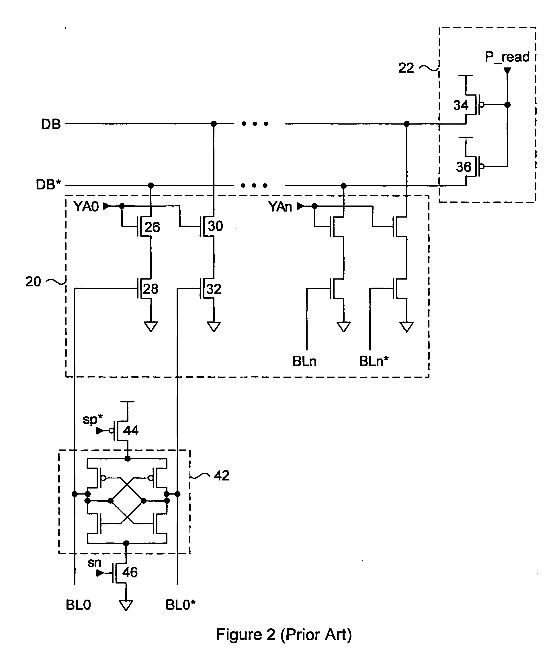
However, this solution requires more complicated bitline sense amplifier control circuitry and requires high voltage devices with thicker oxides, and larger gate lengths.
The additional process cost and area cost may not be acceptable.
However, the disadvantage of supplying the bitline sense amplifier 42 with current from an on-chip regulator is that the sense current capability may be reduced, causing slower bitline operation, even in normal operating modes.
Depending on the architecture and process, this leakage path can also be significant.
Since multiple 2 Mb DRAM macros can be implemented in a system, the total aggregate current leakage can become unacceptable.
However, this configuration results in a slower pull-down of the read databus and requires that the current source for the transistor 46 be large enough to both drive the bitline sense amplifier and pull-down the read databus.

Method used


Image

  • Low power memory architecture
  • Low power memory architecture
  • Low power memory architecture

Examples


Embodiment Construction

[0038] A memory architecture and circuits for minimizing current leakage in the memory array is disclosed. Subdivisions of the memory array each have local power grids that can be selectively connected to global power supply voltages, such that only an accessed subdivision will receive power to execute a requested memory access operation.

[0039]FIG. 4 is a diagram of a memory block implemented with a power distribution scheme according to an embodiment of the present invention. The memory block 100 can be one of several blocks in a memory system, and is composed of a number of subblocks, each labeled 102. Each subblock 102 includes four subarrays, labeled 104, local subblock datapath circuitry 106 and local power gating circuitry 108 for the subblock. As should be appreciated by a person skilled in the art, the memory block 100 can be organized to have a different number and / or organization of subblocks, and each subblock 102 can be organized to have a different number of subbarrays...


PUM


Abstract

A memory architecture and circuits for minimizing current leakage in the memory array. Subdivisions of the memory array each have local power grids that can be selectively connected to power supplies, such that only an accessed subdivision will receive power to execute the memory access operation. The memory array can further include databuses which are precharged to one voltage during idle times and a second voltage during active read cycles, which reduces leakage current in datapath circuitry connected to the databuses within the memory array blocks.

Description

TECHNICAL FIELD [0001] The present invention generally relates to memories. In particular, the present invention relates to low power circuit techniques for memories. BACKGROUND INFORMATION [0002] Semiconductor memories are extensively used in electronics, such as computing devices, mobile devices and other consumer devices. While some memories are used as discrete components, others are embedded with other sub-systems to help realize smaller form-factor mobile devices. For example, microprocessors, digital signal processors (DSP) and application specific integrated circuits (ASIC) have embedded memory. This memory can include volatile memories such as SRAM, DRAM, or non-volatile memories such as Flash memory, for example. [0003] Regardless of the type of memory or how the memory is implemented in the device, an important requirement of the overall system is low power consumption. This requirement is especially important for mobile devices since users prefer to maximize the time the...

Claims


Application Information

Patent Timeline
IPC IPC(8): G11C5/14G11C8/00
CPCG11C5/14G11C2207/065G11C7/1048G11C7/06
Inventor LINES, VALERIE L.
Owner CONVERSANT INTPROP MANAGEMENT INC
Learn More