Sensor device

a sensor device and sensor technology, applied in the direction of instruments, material analysis, and analysis by subjecting materials to chemical reactions, can solve the problems of limited interrogation of the sensing layer, the level of sensitivity and robustness of conventional sensor devices for the detection of chemical stimulus in analyte (e.g. a microanalyte) often fails to provide the level of sensitivity and robustness desired, and limitations are particularly apparent, so as to achieve enhanced signal-to-noise ratio ratio

Inactive Publication Date: 2007-08-30
CROSS GRAHAM +1
View PDF0 Cites 2 Cited by
  • Summary
  • Abstract
  • Description
  • Claims
  • Application Information

AI Technical Summary

Benefits of technology

[0007] Based on the principle of interferometry (which itself is a well established technique), the present invention provides a sensor device which exhibits enhanced signal to noise ratio (sensitivity) by utilising the specialised architecture of a certain sensor component (e.g. a sensor chip) with means (e.g. a microstructure) for intimately exposing the sensor component to a chemical, physical or biological stimulus.

Problems solved by technology

The evanescent component of the optical signal being guided by the waveguide structure is typically small leading to limited interrogation of the sensing layer.
Conventional sensor devices for the detection of a chemical stimulus in an analyte (e.g. a microanalyte) frequently fail to provide the level of sensitivity and robustness desired.
These limitations are particularly apparent with nanolitre quantities of analyte (e.g. microanalytes such as reactants and products).

Method used


Image

  • Sensor device
  • Sensor device
  • Sensor device

Examples


Embodiment Construction

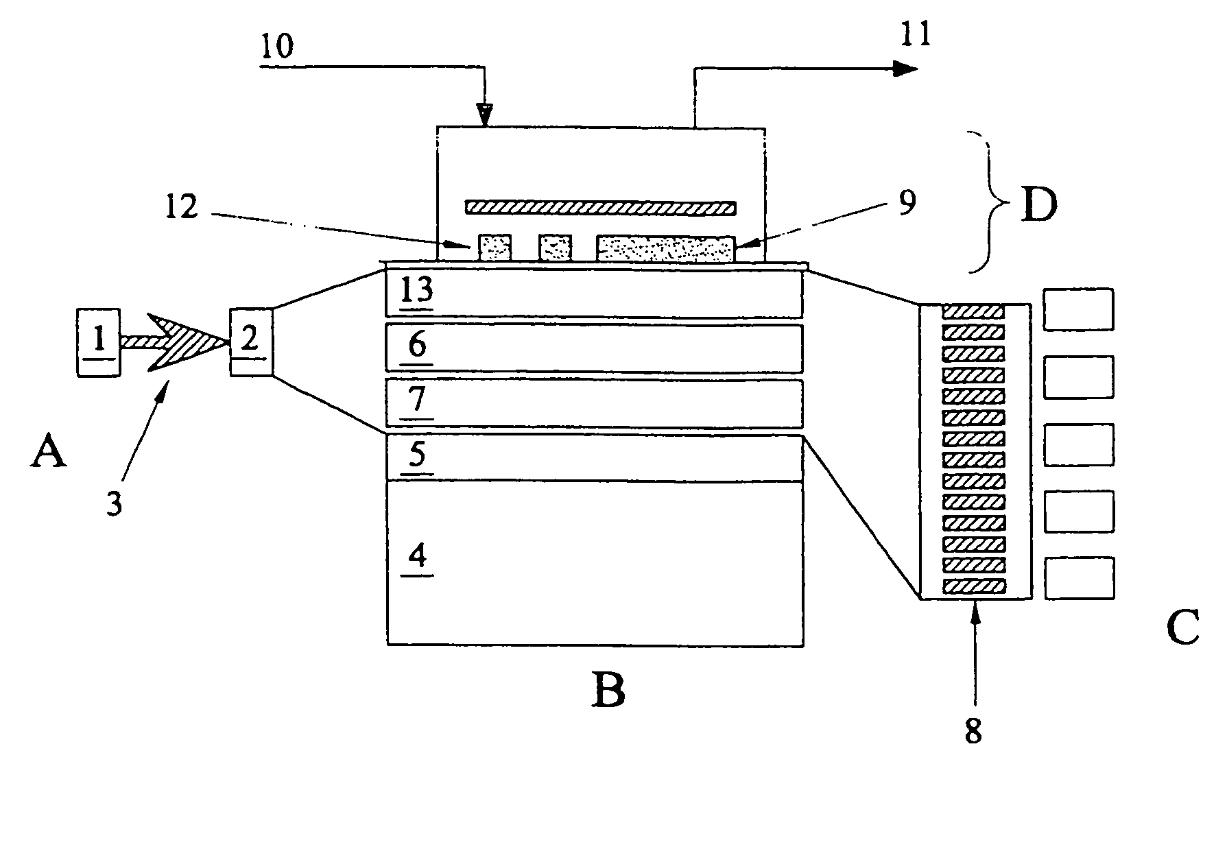
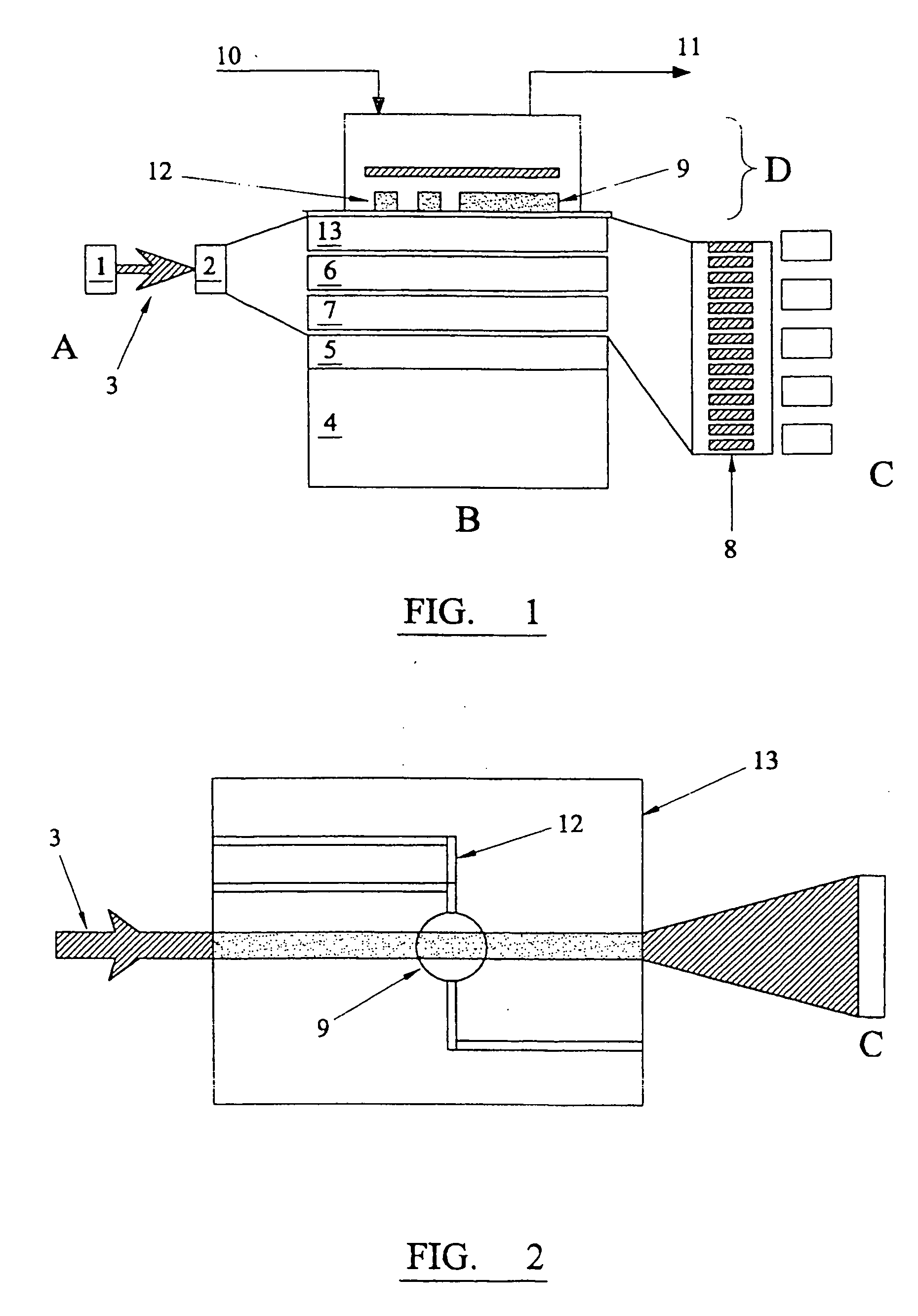
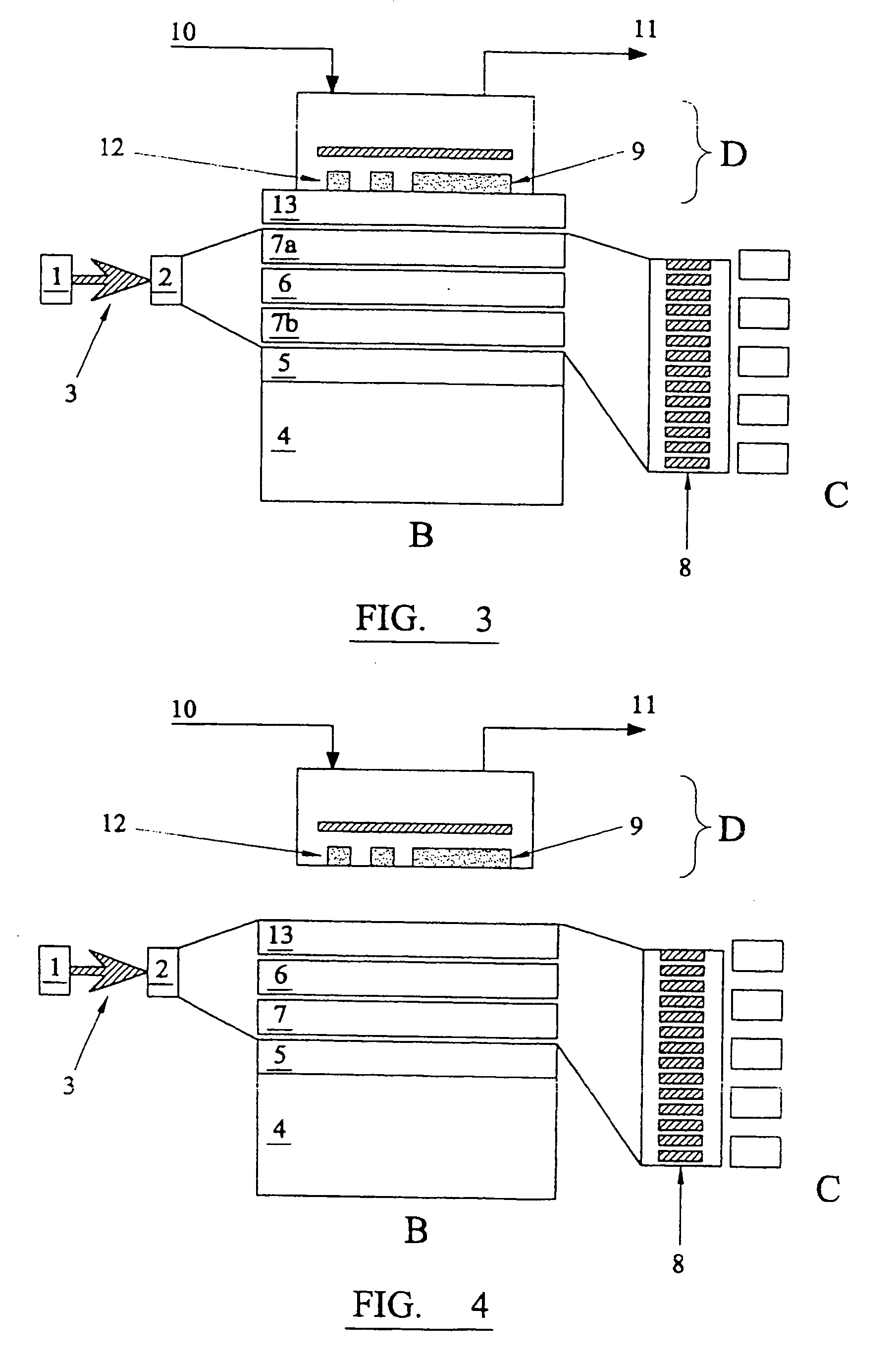
[0074] An embodiment of the sensor device of the invention is shown schematically in FIG. 1 in whole waveguide mode. The sensor device comprises a sensor chip B with a microstructure D integrated onto its upper surface.

[0075] Plane polarised electromagnetic radiation 3 is generated by an electromagnetic source (not shown). The electromagnetic radiation 3 is focussed using a lens 1 (or similar micro-focussing object) and oriented as desired using a polariser 2. The electromagnetic radiation passes into and through the multi-layered structure of the sensor chip B which in this embodiment comprises a silicon layer 4, silicon dioxide layers 5 and 6, a silicon oxynitride layer 7 and an absorbent layer 13. The silicon oxynitride layer 7 acts as the reference waveguide and the absorbent layer 13 as the sensing waveguide.

[0076] The electromagnetic radiation is transmitted into the sensing waveguide 13 and the reference waveguide 7 simultaneously. The layered structure of the sensor chip B...


PUM

PropertyMeasurementUnit
thicknessaaaaaaaaaa
microstructureaaaaaaaaaa
chemical stimulusaaaaaaaaaa

Abstract

The present invention relates to a sensor device for detecting the amount of or changes in chemical stimuli in a gaseous or liquid phase analyte (e.g. a microanalyte) having means for intimately exposing at least a part of the (or each) sensing element to the localised environment containing the chemical stimuli.

Description

CROSS REFERENCE TO RELATED APPLICATION [0001] This application is a continuation of U.S. application Ser. No. 10 / 130,494 filed Jun. 12, 2002 entitled “Sensor Device.”BACKGROUND OF THE INVENTION [0002] 1. Field of the Invention [0003] The present invention relates to a sensor device and method for detecting the amount of (e.g. concentration) or changes in a chemical, physical or biological stimulus of interest in a localised environment, in particular to a sensor device and method for detecting the amount of or changes in chemical stimuli in a gaseous or liquid phase analyte (e.g. a microanalyte). [0004] 2. Background Art [0005] Generally speaking, it is known to make use of the evanescent field component of electromagnetic radiation incident on a waveguide structure (i.e. the field which extends outside the guiding region) to sense discrete changes in optical properties (see inter alia GB-A-2228082, U.S. Pat. No. 5,262,842, WO-A-97 / 12225 and GB-A-2307741). This method relies on “lea...

Claims


Application Information

Patent Timeline
Patent Type & Authority Applications(United States)
IPC IPC(8): G02B6/00G01N33/543G01N21/45G01N21/55G01N21/77
CPCG01N21/45G01N2021/7779G01N21/7703
Inventor CROSS, GRAHAMFREEMAN, NEVILLE JOHN
Owner CROSS GRAHAM
Why Eureka
Try Eureka