Method of manufacturing a semiconductor device

a manufacturing method and technology of a semiconductor device, applied in the direction of semiconductor devices, diodes, electrical devices, etc., can solve problems such as abnormal leakag

Active Publication Date: 2007-09-06
RENESAS ELECTRONICS CORP
View PDF3 Cites 44 Cited by
  • Summary
  • Abstract
  • Description
  • Claims
  • Application Information

AI Technical Summary

Benefits of technology

[0033]An advantage available by the typical invention, of those disclosed by the present application, will next be described.
[0034]Prior to the formation of the first gate electrode of the first MISFET and the second gate electrode of the second MISFET by processing, respective conductor films for the formation of a first gate electrode and a second gate electrode are formed. Processing for the formation of the first gate electrode and second gate electrode is carried out after formation of these conductor films so that the reliability of the first MISFET and the second MISFET can be improved.

Problems solved by technology

The EEPROM having a polysilicon film as a charge storage film has, however, a problem that since the charge storage film is a conductor, a defect in only a portion of an oxide film encompassing the polysilicon film leads to abnormal leakage and all the electrons accumulated in the charge storage film are escaped from the charge storage film.

Method used


Image

  • Method of manufacturing a semiconductor device
  • Method of manufacturing a semiconductor device
  • Method of manufacturing a semiconductor device

Examples


embodiment 1

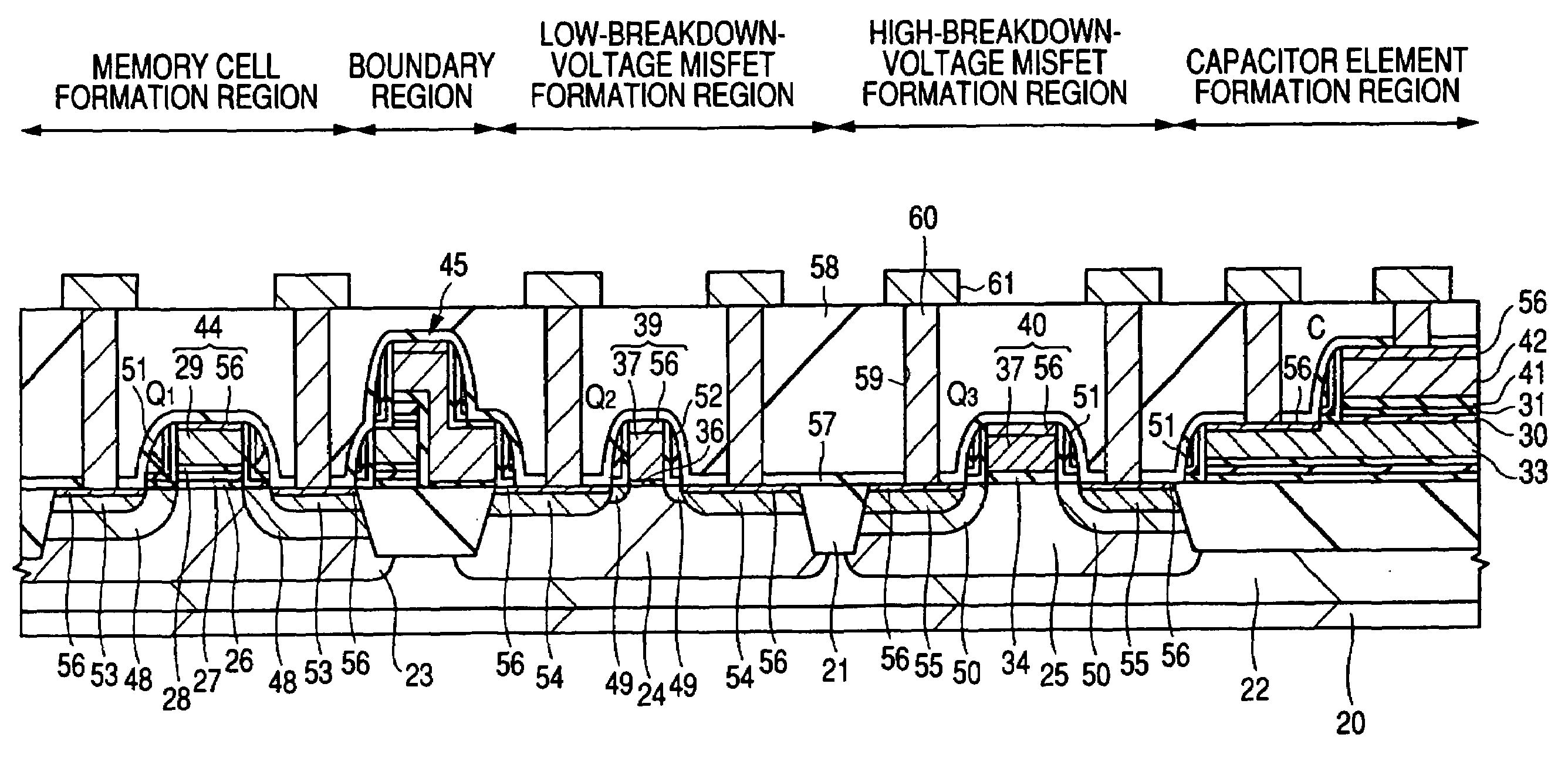
[0090]In Embodiment 1, the present invention is applied to a semiconductor device equipped with a low breakdown voltage MISFET (Metal Insulator Semiconductor) which is driven at a relatively low voltage and a high breakdown voltage MISFET which is driven at a relatively high voltage to enable high-voltage operation and having a programmable nonvolatile memory; and a manufacturing method thereof. In the MISFET, the term “breakdown voltage” means a pn junction breakdown voltage which will be generated at the boundary between a source region and a semiconductor substrate (well) or between a drain region and the semiconductor substrate (well) constituting the MISFET, or a withstand voltage of a gate insulating film. In Embodiment 1, a high breakdown voltage MISFET having a relatively high breakdown voltage and a low breakdown voltage MISFET having a relatively low breakdown voltage are formed over one semiconductor substrate.

[0091]The constitution of the semiconductor device in this Emb...

embodiment 2

[0172]In Embodiment 1, when the gate electrode 39 of the low breakdown voltage MISFET and the gate electrode 40 of the high breakdown voltage MISFET are formed, all of the gate insulating film 34, polysilicon film 37 and cap insulating film 38 are removed from the memory cell formation region. In Embodiment 2, on the other hand, described is an example of leaving the gate insulating film 34, polysilicon film 37 and cap insulating film 38 in the MONOS transistor formation region of the memory cell formation region when the gate electrodes 39 and 40 are formed.

[0173]The manufacturing method of the semiconductor device according to Embodiment 2 is similar to that of Embodiment 1 in the steps illustrated in FIGS. 5 to 11. Then, as illustrated in FIG. 19, the gate electrode 39 and the gate electrode 40 are formed in the low breakdown voltage MISFET formation region and the high breakdown voltage MISFET formation region, respectively, by using photolithography and etching. At this time, a...

embodiment 3

[0179]In Embodiment 1, described was an example of forming the gate electrode 44 of the MONOS transistor after formation of the gate electrode 39 of the low breakdown voltage MISFET and the gate electrode 40 of the high breakdown voltage MISFET. In Embodiment 3, an example of forming the gate electrode 44 of the MONOS transistor, followed by the formation of the gate electrode 39 of the low breakdown voltage MISFET and the gate electrode 40 of the high breakdown voltage MISFET will be described.

[0180]In Embodiment 3, the memory cell formation region corresponds to the second region, while the low breakdown voltage MISFET formation region and high breakdown voltage MISFET formation region correspond to the first region. In other words, the MONOS transistor corresponds to the second MISFET and the low breakdown voltage MISFET and high breakdown voltage MISFET correspond to the first MISFET.

[0181]A step in the manufacturing method of the semiconductor device according Embodiment 3 is s...


PUM


Abstract

Provided is a manufacturing method of a semiconductor device, which comprises forming a film stack of a gate insulating film, a charge storage film, insulating film, polysilicon film, silicon oxide film, silicon nitride film and cap insulating film over a semiconductor substrate; removing the film stack by photolithography and etching from a low breakdown voltage MISFET formation region and a high breakdown voltage MISFET formation region; forming gate insulating films, polysilicon film and cap insulating film over the semiconductor substrate, forming a gate electrode in the low breakdown voltage MISFET formation region and high breakdown voltage MISFET formation region, and then forming a gate electrode in a memory cell formation region. By the manufacturing technology of a semiconductor device for forming the gate electrodes of a first MISFET and a second MISFET in different steps, the present invention makes it possible to provide the first MISFET and the second MISFET each having improved reliability.

Description

CROSS-REFERENCE TO RELATED APPLICATION[0001]The present application claims priority from Japanese patent application No. 2006-54637 filed on Mar. 1, 2006, the content of which is hereby incorporated by reference into this application.BACKGROUND OF THE INVENTION[0002]The present invention relates to a manufacturing technology of a semiconductor device, particularly to a technology effective when applied to the manufacture of the gate electrode of a first MISFET and the gate electrode of a second MISFET by different steps.[0003]In Japanese Unexamined Patent Publication No. 2004-40041, disclosed is a technology of forming, over one semiconductor substrate, both a low-voltage transistor which operates at a low voltage and a flash memory which operates at a high voltage and has a two-layer electrode structure called ETOX.[0004]Described specifically, both a field oxide film for element isolation and a protection oxide film for ion implantation are formed over a semiconductor substrate in...

Claims


Application Information

Patent Timeline
Patent Type & Authority Applications(United States)
IPC IPC(8): H01L21/8238
CPCH01L21/823462H01L27/0629H01L27/1052H01L27/11568H01L27/11573H01L27/105H10B99/00H10B43/40H10B43/30
Inventor TANIGUCHI, YASUHIROSHIBA, KAZUYOSHI
Owner RENESAS ELECTRONICS CORP
Why Eureka
Try Eureka