
Thin multichip flex-module

a multi-chip, flexible technology, applied in the direction of printed circuit manufacturing, printed circuit construction, electrical apparatus construction details, etc., can solve the problems of reducing manufacturing costs, reducing manufacturing efficiency, and limiting technology to low volume, so as to improve manufacturing efficiency and improve component and interconnect density. density

Inactive Publication Date: 2007-09-13
MICROELECTRONICS ASSEMBLY TECH
View PDF25 Cites 114 Cited by
  • Summary
  • Abstract
  • Description
  • Claims
  • Application Information

AI Technical Summary

Benefits of technology

[0009]Objects of the present invention include providing an improved memory module design that uses bare die or chip-scale packaged (CSP) memory chips; providing a method by which memory modules can be produced in higher volumes than modules built on PCB panels using surface mount soldering; providing a memory module that is cheaper to manufacture than modules built on PCB panels using surface mount soldering; providing a memory module that can be actively cooled; providing a memory module having higher component and interconnect density; and, providing an improved method for manufa

Problems solved by technology

Unfortunately, this technology is currently too expensive for most of these applications.
A principal reason for the expense associated with multichip modules is that the technology is constrained to low volume, custom applications which cannot attain sufficient market volumes to help drive manufacturing costs down.
Part of this problem is exacerbated by a current shortage of reliable, high-volume sources for the large variety of “known good die” required by many MCM applications.
However, identifying and implementing a high-volume, industry standard MCM application is still proving elusive.
Hence, the standard memory module business is widely thought to be too cost-driven to be considered a good candidate for MCM technology.
None of the foregoing discloses means for cooling the interior of the modules.

Method used


Image

  • Thin multichip flex-module
  • Thin multichip flex-module
  • Thin multichip flex-module

Examples


Embodiment Construction

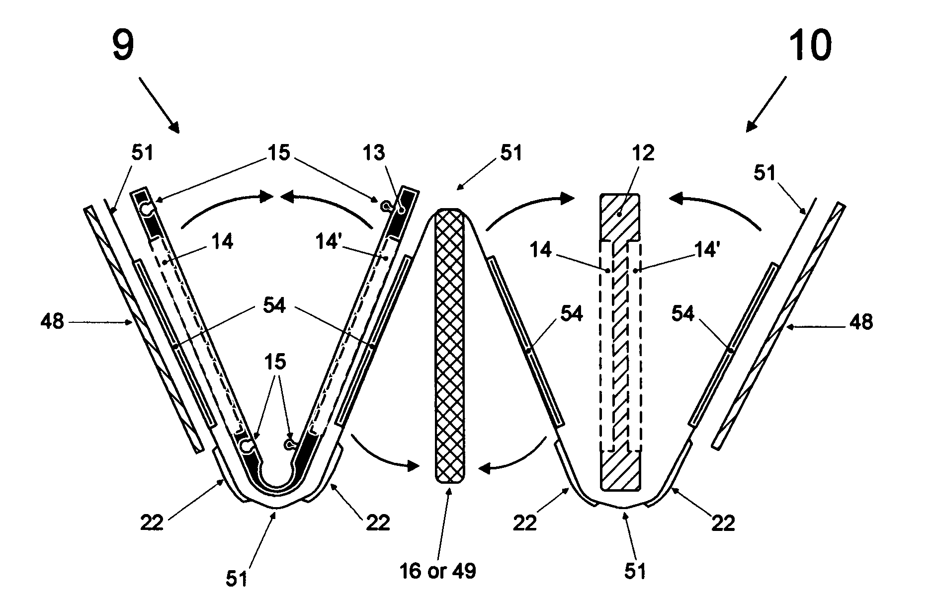
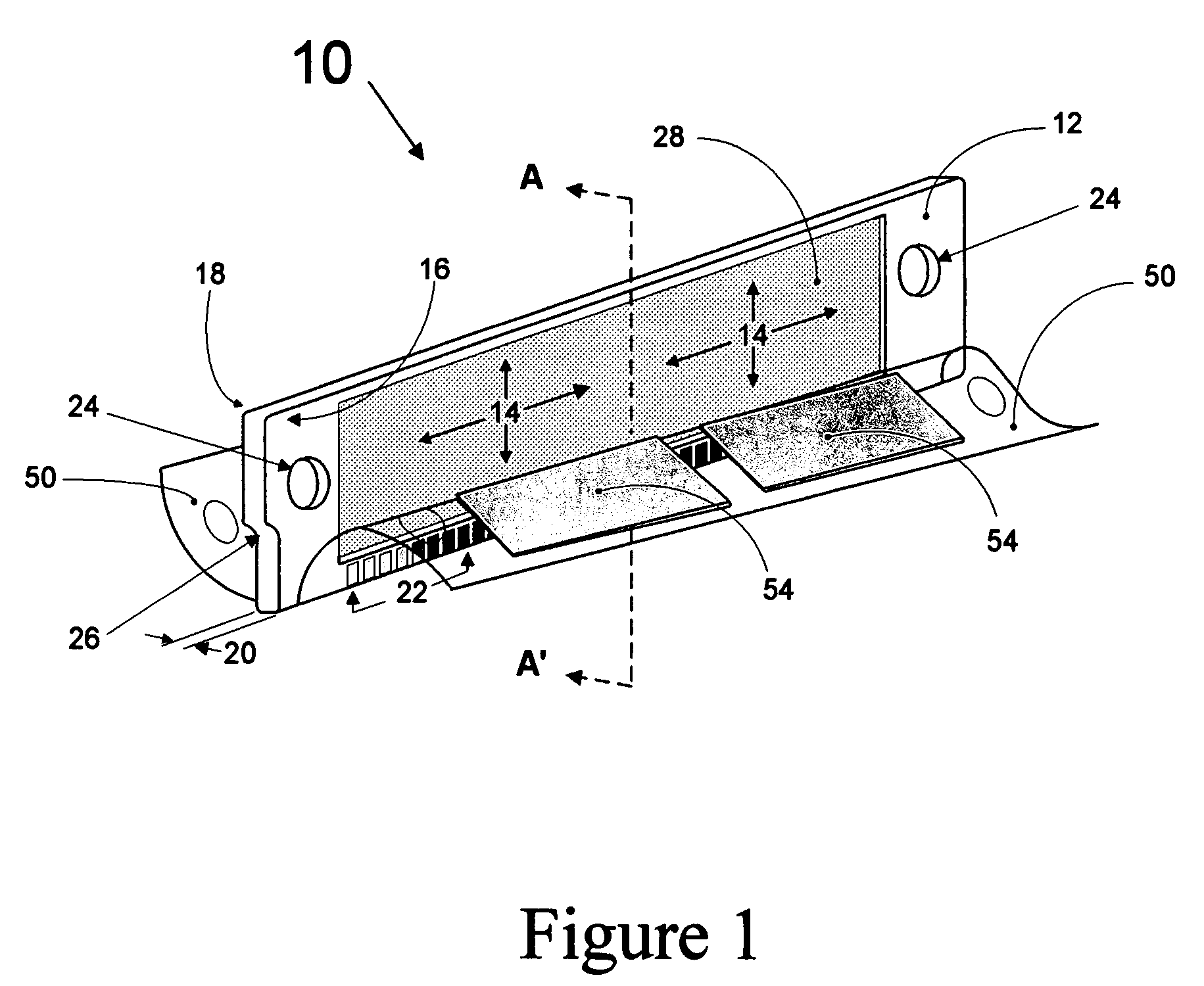
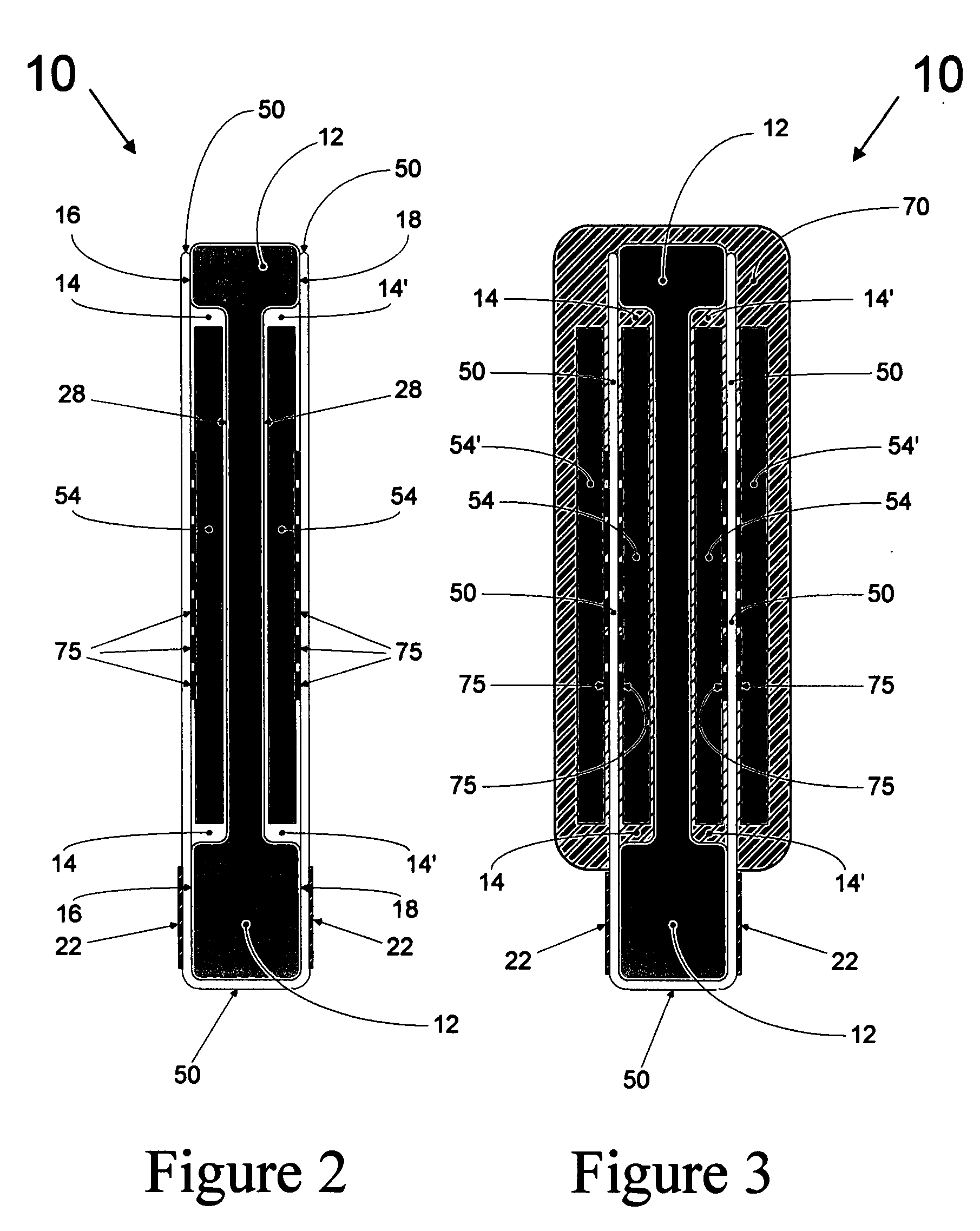
[0048]The following embodiments introduce new construction concepts and assembly methods directed at providing lower-cost, higher-density, packaging solutions for next generation electronic module products. The module embodiments disclosed herein may be broadly classified as “Multichip Modules” in that the semiconductor devices illustrated are preferably in a “bare-die” or “chip” form. It will be understood, however, that in some instances packaged die may be used instead of bare die, depending on design objectives.

[0049]The electronics industry presently recognizes three main types or divisions of multichip modules based on the type of interconnecting substrate upon which the bare-die or chips are assembled: MCM-D (deposited thin film), MCM-C (ceramic), and MCM-L (laminate). MCM type-L refers to conventional epoxy / glass, printed circuit board laminate substrates and comes closest, of the three categories, for classifying the present invention. Epoxy / glass PCBs, however, are general...


PUM


Abstract

A multichip module comprises: a first rigid member defining one outer wall of a chamber; a second rigid member defining the opposite wall of the chamber; a sealable interface joining the first and second rigid members at their peripheries, whereby a hollow chamber is formed; a flex circuit having a plurality of integrated circuit chips disposed thereon, the flex circuit affixed to at least one of the first and second rigid members; electrical contacts at least partially extending outward through the sealable interface; and, a fluid inlet and a fluid outlet configured to permit fluid to flow through the chamber whereby heat generated by the integrated circuit chips may be removed from the module.

Description

CROSS-REFERENCE TO RELATED APPLICATION[0001]This application claims the benefit of Provisional Patent Application No. 60 / 780,440 by the present inventors, filed on Mar. 8, 2006, the entire disclosure of which is incorporated herein by reference.BACKGROUND OF THE INVENTION[0002]1. Field of the Invention[0003]The present invention relates generally to means for packaging microelectronic devices. More particularly, the invention relates to improved, SIMM and DIMM type memory modules.[0004]2. Description of Related Art[0005]Multichip module (MCM) assembly is currently an enabling technology for improving system performance in high-end workstation and super computers. By interconnecting multiple bare dice on a single substrate, packaging density is increased and chip-to-chip communication distance is consequently shortened, enabling higher operating speeds. Small, lightweight consumer products such as notebook or handheld computers and telephony products are expected to benefit from the ...

Claims


Application Information

Patent Timeline
IPC IPC(8): H05K7/20
CPCH01L23/473H01L23/5387H01L2924/0002H01L2225/06589H01L2924/09701H01L2924/3011H05K1/189H05K3/0061H05K3/0064H05K2201/056H05K2201/064H05K2201/09445H05K2201/2018H01L2924/00
Inventor CLAYTON, JAMES E.FATHI, ZAKARYAE
Owner MICROELECTRONICS ASSEMBLY TECH
Features
  • Generate Ideas
  • Intellectual Property
  • Life Sciences
  • Materials
  • Tech Scout
  • Unparalleled Data Quality
  • Higher Quality Content
  • 60% Fewer Hallucinations
Learn More