Gas Discharge Display Panel

a display panel and gas discharge technology, applied in the manufacture of electric discharge tubes/lamps, cold cathode manufacture, electrode systems, etc., can solve the problems of discharge delay, characteristic change of protective layer, and easy “discharge delay” of conventional protective layers, so as to reduce the starting voltage of discharge and low cost

Inactive Publication Date: 2007-09-20
PANASONIC CORP
View PDF3 Cites 17 Cited by
  • Summary
  • Abstract
  • Description
  • Claims
  • Application Information

AI Technical Summary

Benefits of technology

[0036] The inventors of the present invention have been dedicated to finding a method of solving the conventional problem of discharge delay in the address period. As a result, the inventors have found that the problem is solved by making a protective layer by including, in the main component of MgO, Si, or Ge respectively in the above-defined content ratio, and optionally H.
[0037] According to the protective layer having the stated structures, by the addition of the Si, Ge, and H respectively in an adequate amount to MgO, it becomes possible to produce such advantageous effects as enabling to control the discharge delay in an optimal range without lowering the wall charge retaining power at the time of driving, and to dramatically and effectively prevent the occurrence of writing defect during the address period. Furthermore, the protective layer having the stated structures also lowers the discharge starting voltage.
[0038] In addition, the present invention has another advantage of being realized in comparatively low cost, because of the structure of merely adding Si, Ge, and optionally H respectively in an adequate amount to MgO.

Problems solved by technology

The first problem is that conventional protective layers are susceptible to “discharge delay”.
If the discharge delay is large, the possibility of preventing address discharge from occurring even at the end of the address pulse application becomes high, with which writing defect is likely caused.
The problem of discharge delay is a problem to be solved for improving image display performance of PDPs.
The second problem is a characteristic change of the protective layer.
In a process performed in the air from among the PDP manufacturing processes, a protective layer made of MgO tends to be contaminated by absorption of oil impurity, CO2, and H2O.
When the absorption gas is absorbed by the surface of the MgO, the characteristic of the protective layer changes, thereby decreasing the secondary electron emission efficiency.
This would lead to a problem of display defect called “black noise” which specifically is a phenomenon in which accurate display of intended cells is impaired.

Method used


Image

  • Gas Discharge Display Panel
  • Gas Discharge Display Panel
  • Gas Discharge Display Panel

Examples


first embodiment

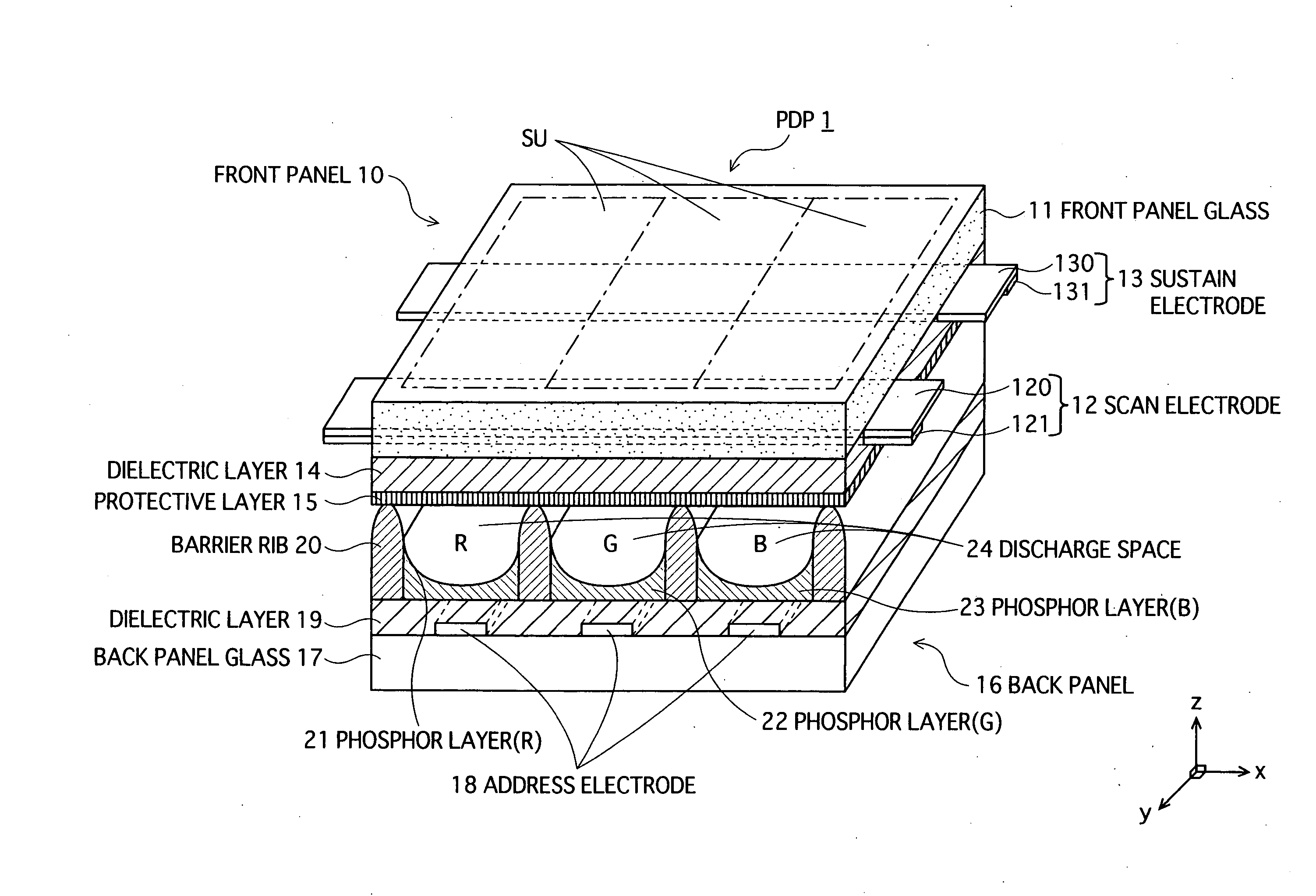
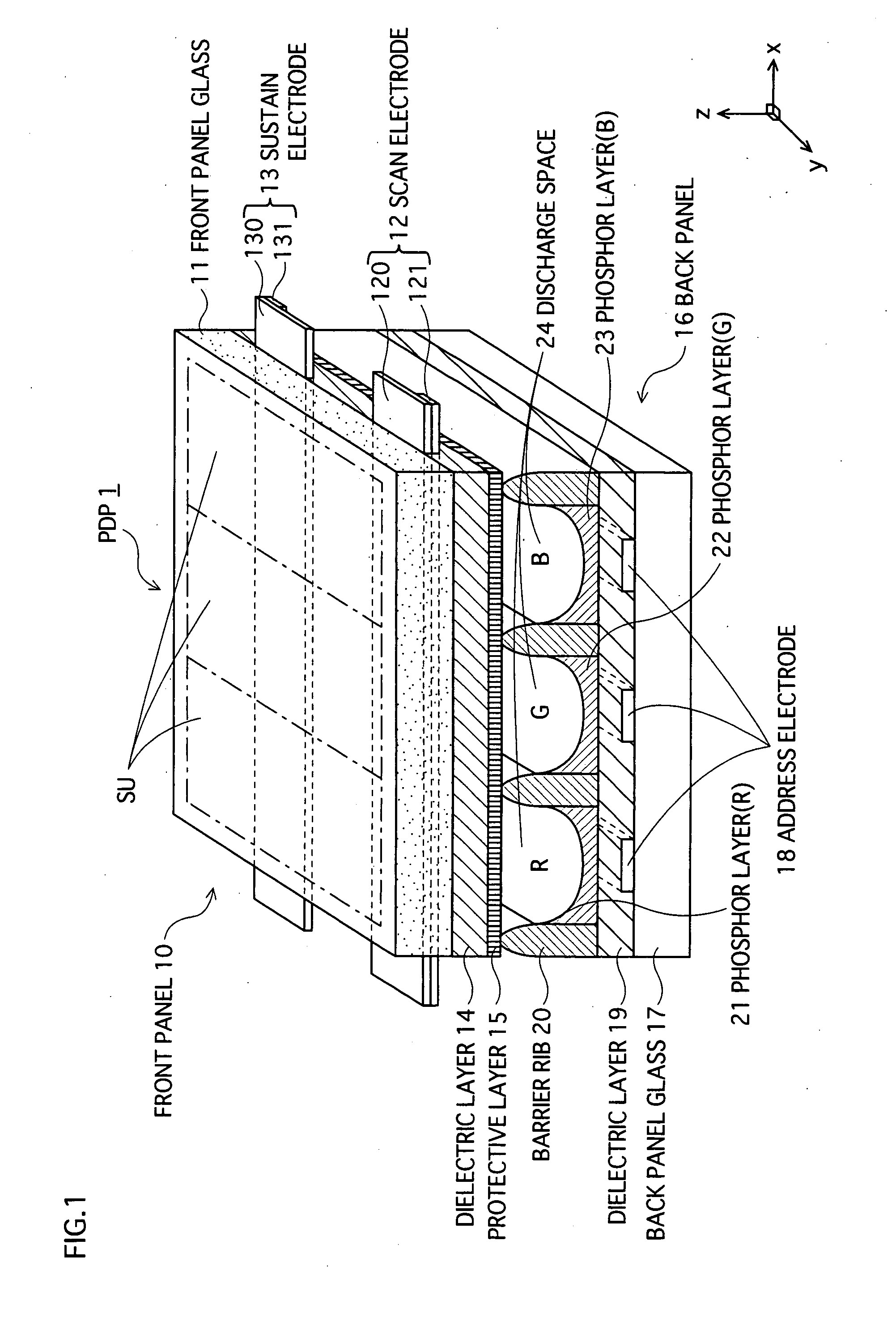
[0040] 1-1. Structure of PDP

[0041]FIG. 1 is a partial perspective view showing a main structure of an AC-type PDP 1, according to the first embodiment of the present invention. In the drawing, the z-direction corresponds to a thickness direction of the PDP 1, and the xy plane corresponds to a plane parallel to the surface of the panels of the PDP 1. Here, the PDP 1 has an NTSC specification of 42 inches for example. However needless to say, the present invention is also applicable to other specifications, including XGA, and SXGA. The present invention is also applicable to other sizes.

[0042] As FIG. 1 shows, the PDP 1 is mainly structured by a front panel 10 and a back panel 16 whose main surfaces are opposed to each other.

[0043] On one main surface of the front panel glass 11 that is a substrate of the front panel 10, a plurality of pairs of display electrodes 12 and 13 (scan electrode 12 and sustain electrode 13) are provided. Each display electrode 12, 13 is formed by stacking...

modification example 1

[0181] In the present modification example 1, first, a film mainly composed of MgO and additionally containing Si or Ge is formed using the method described in the first embodiment.

[0182] Then, means for generating H ion is used as a method of doping the H atoms to the film, thereby irradiating H ion on the surface of the formed film.

[0183] Here, the setting conditions are as follows for example: using a heater, the substrate is heated to the temperature of 100-300 degrees Celsius within the doping chamber of H atoms, and the chamber is evacuated until the vacuum level reaches 1×10⁻⁴-7×10⁻⁴ Pa.

[0184] After this, H ions are irradiated onto the protective layer 15 having been formed on the substrate using an ion gun linked to the H container, thereby doping H atoms of the protective layer 15. The amount of flowing for H is set in the range of 1×10⁻⁵-3×10⁻⁵ m3 / min.

modification example 2

[0185] In the modification example 2, first a film made of MgO is formed using the method described in the first embodiment. Then the formed film is placed in a chamber. While the film is being subjected to plasma processing in the atmosphere containing H, and an evaporation source created by mixing a Si compound and a Ge compound is heated using an electron beam gun, thereby completing a protective layer containing H and either Si or Ge.


PUM

PropertyMeasurementUnit
wavelength rangeaaaaaaaaaa

Abstract

Provided is a gas discharge display panel that exhibits a favorable display performance by maintaining a wall charge retaining power, controlling discharge delay within a range adequate for optimal image display, and reducing the discharge starting voltage at comparatively low cost. Also provided is a PDP that exhibits more reliability with enhanced display quality by further improving the secondary electron emission factor γ compared to conventional cases and lowering the discharge starting voltage to widen the driving margin. In addition, provided is a manufacturing method of a gas discharge display panel, by which the manufacturing cost lowers by reduction of the exhaustion time in the sealing exhaustion process, and by which the driving circuit cost is reduced. In the present invention, the protective layer contains, with respect to a MgO content of the protective layer, Si in a range of 20 mass ppm to 5000 mass ppm inclusive and H in a range of 300 mass ppm to 10000 mass ppm inclusive.

Description

TECHNICAL FIELD [0001] The present invention relates to a gas discharge display panel such as a plasma display panel. The present invention particularly relates to a technology for improving a protective layer. BACKGROUND ART [0002] G as discharge display panels, represented by a plasma display panel (herein after simply “PDP”), are display apparatuses that display images by light emission performed by exciting phosphors by means of ultraviolet light generated by gas discharge. According to the discharge forming method, PDPs are divided into two types of alternating current (AC) type and direct current (DC) type, where the AC type is most common because of superiority over the DC type in terms of brightness, light emission efficiency, and lifetime. [0003] As is disclosed in Patent reference 1 for example, an AC-type PDP has the following structure. Two thin glass panels respectively provided with a plurality of electrodes (either display electrodes or address electrodes) and a diele...

Claims


Application Information

Patent Timeline
Patent Type & Authority Applications(United States)
IPC IPC(8): H01J11/02H01J9/02H01J17/49
CPCH01J11/40H01J11/12C23C14/081H01J11/38
Inventor HASHIMOTO, JUNKITAGAWA, MASATOSHINISHITANI, MIKIHIKOTERAUCHI, MASAHARUYAMAMOTO, SHINICHI
Owner PANASONIC CORP
Why Eureka
Try Eureka