Thin film transistor integrated circuit device, active matrix display device, and manufacturing methods of the same

a technology of integrated circuit and active matrix, which is applied in the direction of transistors, optics, instruments, etc., can solve the problems of increasing the manufacturing cost of active matrix substrates and extremely low material utilization efficiency, and achieves the reduction of the manufacturing cost of the device, the effect of thin film wiring and low cos

Inactive Publication Date: 2007-09-27
ZEON CORP
View PDF9 Cites 16 Cited by
  • Summary
  • Abstract
  • Description
  • Claims
  • Application Information

AI Technical Summary

Benefits of technology

[0031] According to the device of this invention, since the surfaces of the wiring, the source electrodes, and the drain electrodes form substantially the same plane with the flattening layer surrounding them, the flat wiring structure can be achieved without stacking the flattening layer on the signal lines and thus the thick film wiring can be easily achieved. Further, in the case where the flattening layer is formed of a resin, it can be formed without requiring a decompression process such as CVD and, therefore, the manufacturing cost of the device can be reduced.
[0032] Further, according to the manufacturing method of this invention, since use can be made of the printing method such as the inkjet printing method or the screen printing method, or the plating method for forming the wiring, the source electrodes, and the drain electrodes, the display device can be manufactured at low cost and with high yield.
[0033] Further, according to the active matrix display device of this invention, since the structure is flat with no level different shape otherwise caused by the scanning lines and the gate wiring, it is possible to obtain an excellent display with less degradation of the display elements.
[0034] According to this invention, in the active matrix display device having, on the insulating substrate, at least, the scanning lines, the signal lines, and the thin film transistors provided near crossing portions between the scanning lines and the signal lines and each having the gate electrode connected to the scanning line and the source or drain electrode connected to the signal line, since the surfaces of the signal lines, the source electrodes, and the drain electrodes form substantially the same plane with the flattening layer surrounding them, the flat wiring structure can be achieved without stacking the flattening layer on the signal lines and thus the thick film wiring can be easily achieved. Further, in the case where the flattening layer is formed of a resin, it can be formed without requiring a decompression process such as CVD and, therefore, the manufacturing cost of the active matrix display device can be reduced.
[0035] On the other hand, according to the manufacturing method of the active matrix display device of this invention, since use can be made of the printing method such as the inkjet printing method or the screen printing method, or the plating method for forming the signal lines, the source electrodes, and the drain electrodes, the display device can be manufactured at low cost and with high yield.
[0036] Since the active matrix display device of this invention has the flat structure with no level different shape otherwise caused by the scanning lines and the gate wiring, it is possible to obtain an excellent display with less degradation of the display elements and, further, the pixel electrodes can be overlapped with the source and drain electrode wiring so that there is also an effect that the pixel electrodes can be enlarged.

Problems solved by technology

Particularly, the process of forming the wiring by sputtering is a main cause for increasing the manufacturing cost of the active matrix substrate because, since a wiring material formed over the entire surface is processed by a photolithography method to thereby form wiring portions, most of the material is removed by etching and, further, a material target, which is large as compared with the area of the substrate, is used for ensuring uniformity of the film thickness, and therefore, the material utilization efficiency is extremely low.

Method used


Image

  • Thin film transistor integrated circuit device, active matrix display device, and manufacturing methods of the same
  • Thin film transistor integrated circuit device, active matrix display device, and manufacturing methods of the same
  • Thin film transistor integrated circuit device, active matrix display device, and manufacturing methods of the same

Examples


embodiment 1

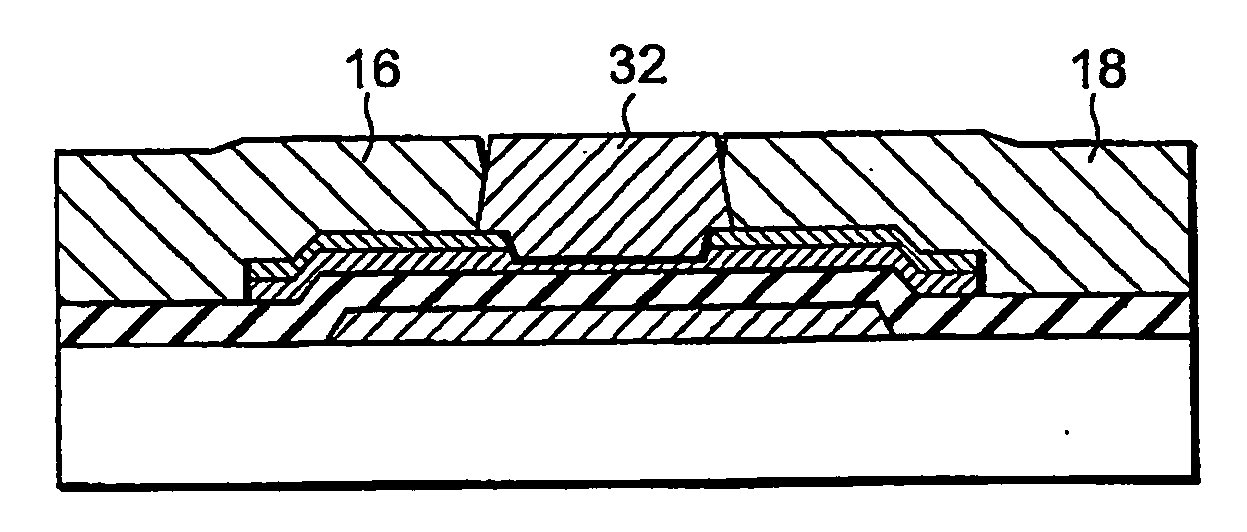
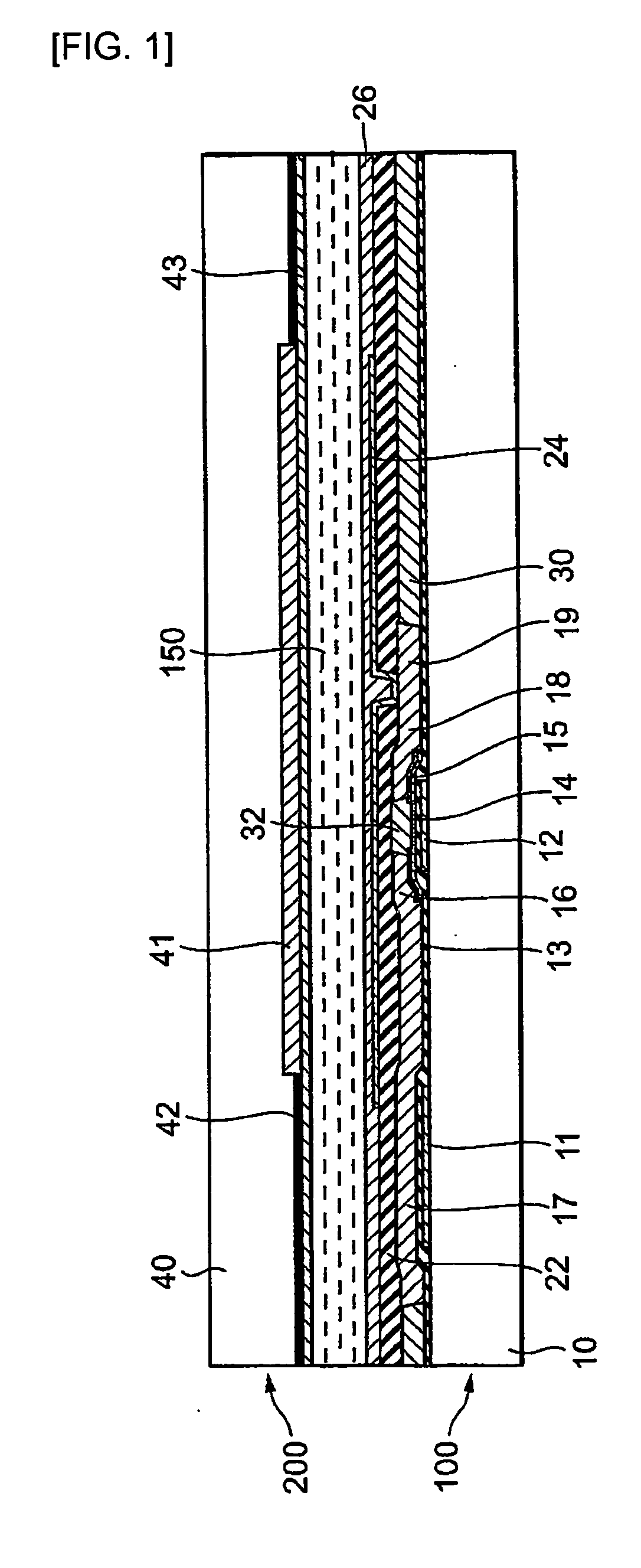
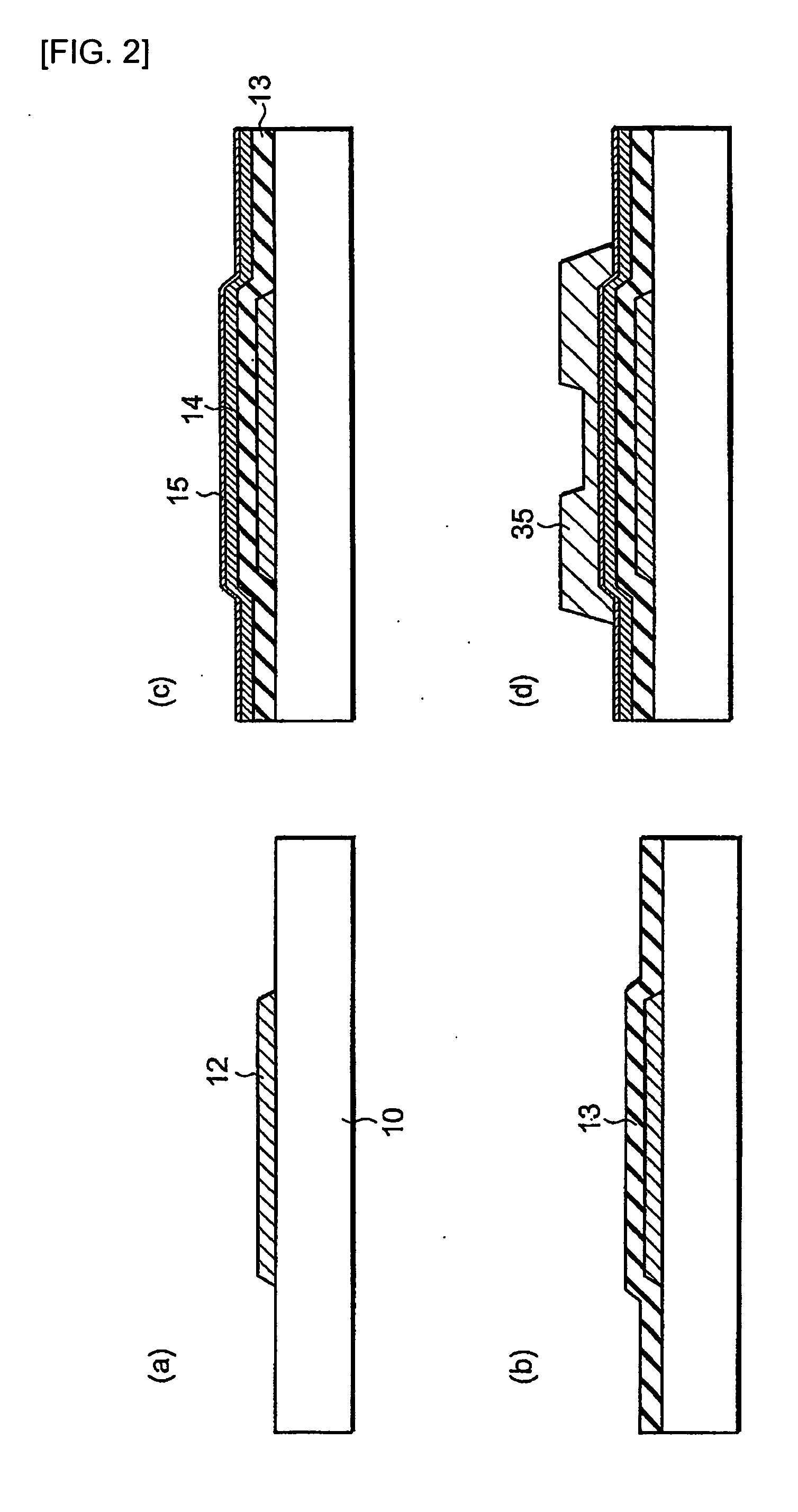
[0045] Referring to FIG. 1, description will be made about an active matrix liquid crystal display device according to Embodiment 1 of this invention. FIG. 1 is a schematic diagram showing a section of the active matrix liquid crystal display device according to this Embodiment 1, wherein the illustrated liquid crystal display device comprises an active matrix substrate (hereinafter referred to as a matrix substrate) 100 and a filter substrate 200 disposed so as to face the matrix substrate 100 through liquid crystals 150. Of them, the matrix substrate 100 comprises a glass substrate 10, a scanning line 11 provided on the glass substrate 10, and a gate electrode 12 connected to the scanning line 11 at a non-illustrated portion. Further, a gate insulating film 13 is formed on the scanning line 11 and the gate electrode 12, and a first semiconductor layer 14 and a second semiconductor layer 15 are formed in a thin film transistor (TFT) forming region of the gate insulating film 13. Am...

embodiment 2

[0066] Referring to FIG. 5, description will be made about an active matrix liquid crystal display device according to Embodiment 2 of this invention. In FIG. 5, the same reference numerals are assigned to portions corresponding to those of the liquid crystal display device shown in FIG. 1. The active matrix liquid crystal display device shown in FIG. 5 differs from the liquid crystal display device shown in FIG. 1 in that a scanning line 11 and a gate electrode 12 formed on a glass substrate 10 are embedded in an insulating film 45 and, as a result, the scanning line 11, the gate electrode 12, and the insulating film 45 also form substantially the same plane and a gate insulating film 13 is uniformly formed on this flattened surface.

[0067] Also in FIG. 5, the gate electrode 12 is connected (not shown) to the scanning line 11 near a crossing portion between the scanning line 11 and a signal line 17 and a source or drain electrode 16 or 18 is connected to the signal line 17 on the g...

embodiment 3

[0073] In Embodiment 3 of this invention, an active matrix organic EL display device was formed according to a technique like that used in Embodiments 1 and 2. FIG. 7 is a sectional view showing a structure of the formed organic EL display device, wherein, for the sake of explanation, the same reference numerals are assigned to those portions having equivalent functions in FIGS. 1 and 5. The organic EL display device shown in FIG. 7 has a scanning line 11 and a gate electrode 12 formed on a glass substrate 10 and, like in FIG. 5, the illustrated scanning line 11 and gate electrode 12 are embedded in an insulating film 45. As described with reference to FIG. 6, a transparent photosensitive resin can be used as the insulating film 45.

[0074] Further, in the illustrated example, a gate insulating film 13 is formed on the scanning line 11, the gate electrode 12, and the insulating film 45, which forms the flat surface, and first and second semiconductor layers 14 and 15, source and drai...


PUM

PropertyMeasurementUnit
thicknessaaaaaaaaaa
thicknessaaaaaaaaaa
temperatureaaaaaaaaaa

Abstract

There is provided an active matrix display device including a flattening layer formed so as to surround a source electrode wiring, a drain electrode wiring, and a signal line, so that the source electrode wiring, the drain electrode wiring, and the signal line form substantially the same surface with the flattening layer.

Description

TECHNICAL FIELD [0001] This invention relates to a thin film transistor integrated circuit device and further relates to an active matrix display device using thin film transistors (TFTS) and manufacturing methods thereof. BACKGROUND ART [0002] A thin film transistor integrated circuit device constitutes a microprocessor, a system LSI (large scale integration) circuit, or the like by disposing, on an insulator substrate such as a glass substrate or on a substrate of which at least the surface is an insulator, many thin film transistors and a single wiring layer or multiple wiring layers adapted to connect those transistors to each other and to a power supply and input / output terminals. As one of its embodiments, there is an active matrix display device such as an active matrix liquid crystal display device or an organic EL (electroluminescence) display device. The active matrix display device basically has pixels arranged in a matrix, thin film transistors (hereinafter abbreviated a...

Claims


Application Information

Patent Timeline
Patent Type & Authority Applications(United States)
IPC IPC(8): G02F1/1333G02F1/136G02F1/1368H01L21/336H01L21/77H01L27/12H01L29/417H01L29/786
CPCG02F1/1368G02F2001/133357H01L27/12H01L29/41733H01L27/1292H01L29/78636H01L27/124H01L27/1248H01L27/1285H01L29/66742G02F1/133357H01L27/1214
Inventor OHMI, TADAHIRO
Owner ZEON CORP
Why Eureka
Try Eureka