Plasma processing method and plasma processing apparatus

a plasma processing and plasma technology, applied in the field of plasma processing methods, can solve the problems of considerable deterioration of the in-surface uniformity of the process, and achieve the effects of ensuring enhancing the uniformity of the process, and maintaining stably the uniformity of the plasma processing

Active Publication Date: 2007-10-04
TOKYO ELECTRON LTD
View PDF12 Cites 188 Cited by
  • Summary
  • Abstract
  • Description
  • Claims
  • Application Information

AI Technical Summary

Benefits of technology

[0019]In accordance with the third and the fourth aspect of the present invention, the electrostatic capacitance of the capacitance varying unit is controlled based on the number of plasma-processed substrates, so that the spatial density distribution of the plasma and the in-surface variance of the process can be controlled. Thus, the uniformity of the process can be stably secured.
[0020]It is preferable that the capacitance control unit sets the electrostatic capacitance of the capacitance varying unit to be high in advance, and to be reduced as the number of substrates on which the plasma process is performed increases.
[0021]In accordance with the plasma processing method and the plasma processing apparatus of the present invention, with the configurations and functions described above, deposits can be prevented from being attached to an electrode on an anode side and thus affecting the subsequent processes in a cathode coupling arrangement, and the uniformity of the process can be enhanced. Further, even if a change in processing environments occurs with a lapse of time as the plasma processing is repeatedly performed, the uniformity of the plasma processing can be stably maintained.

Problems solved by technology

As a result, there occurs a problem that an in-surface uniformity of the process is considerably deteriorated.

Method used


Image

  • Plasma processing method and plasma processing apparatus
  • Plasma processing method and plasma processing apparatus
  • Plasma processing method and plasma processing apparatus

Examples


Embodiment Construction

[0032]Hereinafter, embodiments of the present invention will be described with reference to the accompanying drawings.

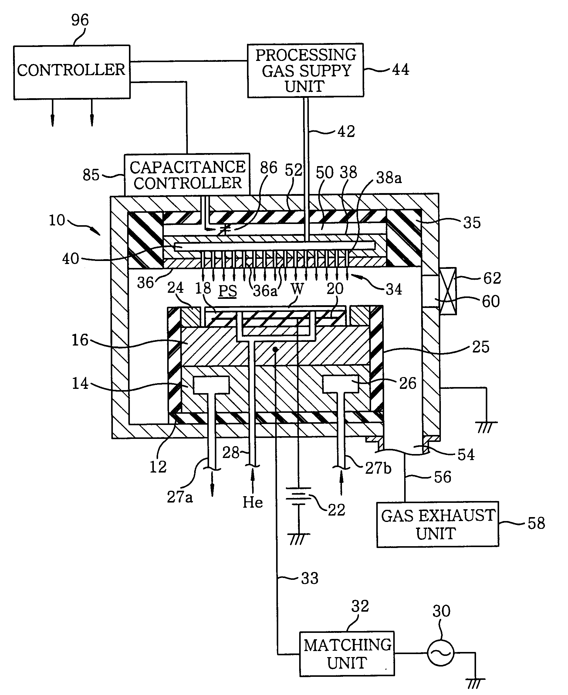
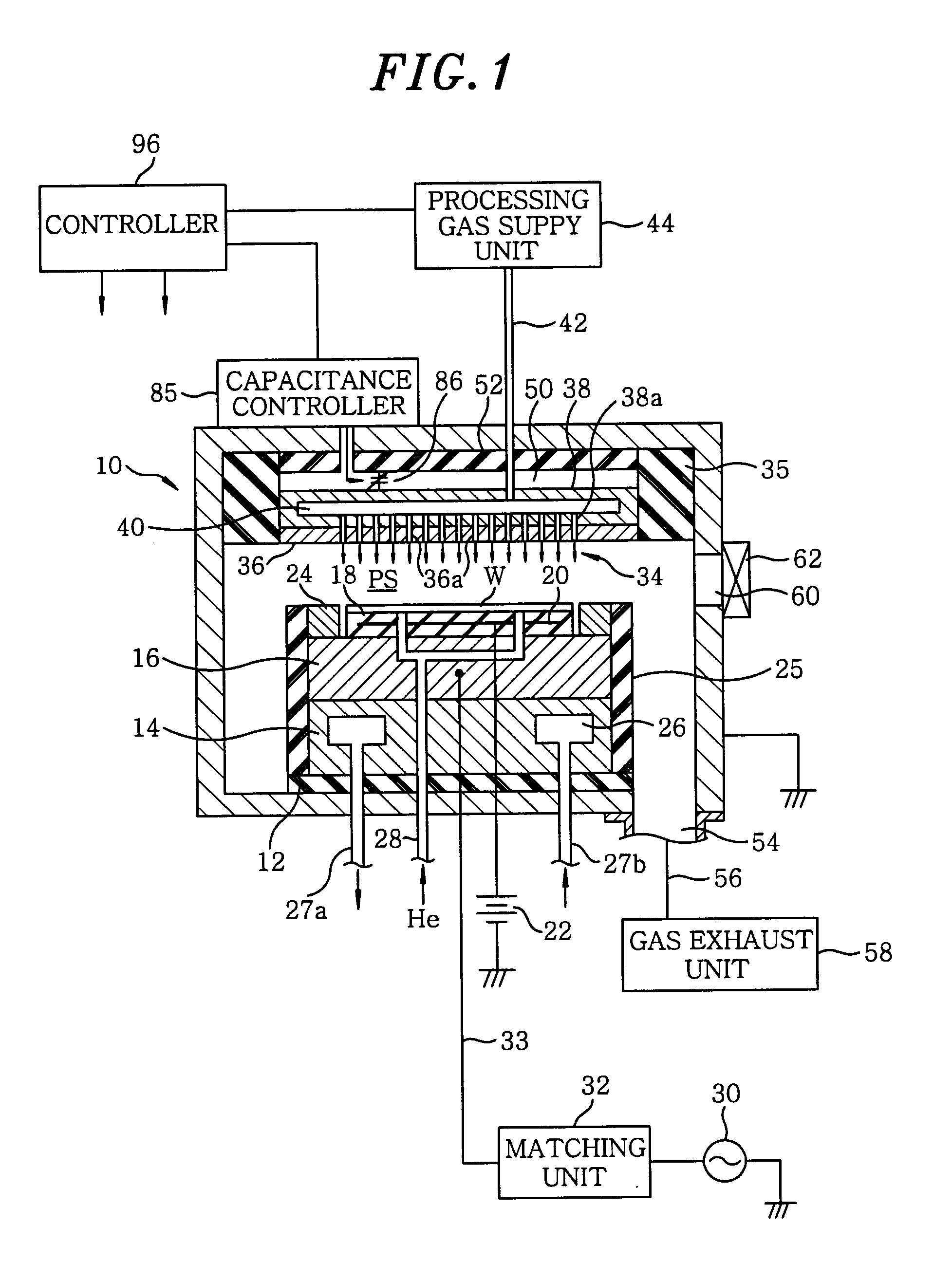
[0033]FIG. 1 illustrates a configuration of a plasma processing apparatus in accordance with an embodiment of the present invention. The plasma processing apparatus is configured as a capacitively coupled (parallel plate type) plasma processing apparatus of a cathode coupling type. The plasma processing apparatus has a cylindrical vacuum chamber (processing chamber) 10 made of, e.g., an aluminum whose surface is alumite-treated (anodically oxidized), and the chamber 10 is frame grounded.

[0034]A cylindrical susceptor support 14 is provided at a bottom portion in the chamber 10 via an insulation plate 12 made of ceramic or the like. Further, a susceptor 16 made of, e.g., aluminum, is disposed above the susceptor support 14. The susceptor 16 serves as a lower electrode and a target substrate, e.g., a semiconductor wafer W, is mounted thereon.

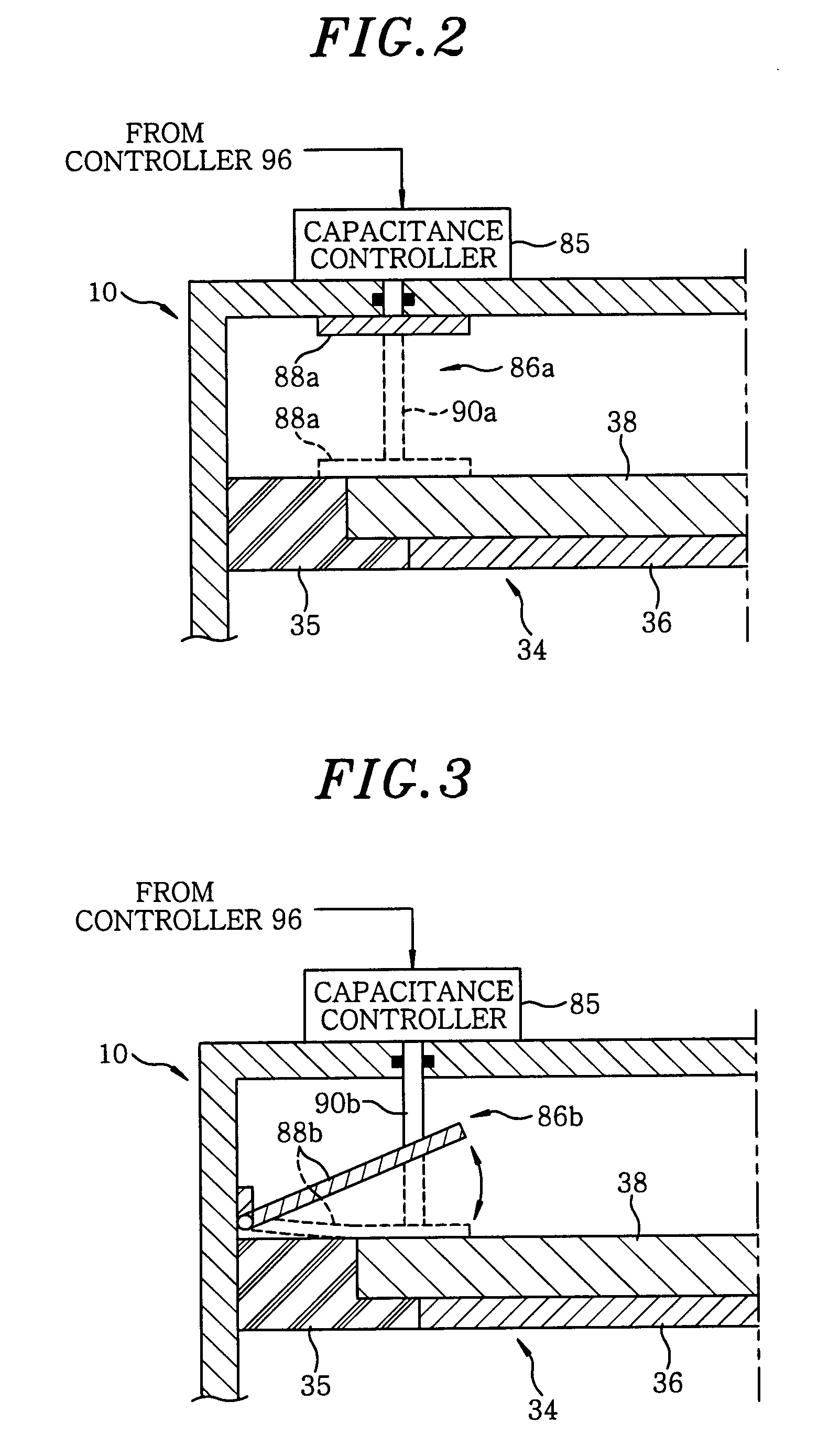
[0035]On the top surface of ...


PUM

PropertyMeasurementUnit
frequencyaaaaaaaaaa
frequencyaaaaaaaaaa
capacitanceaaaaaaaaaa

Abstract

A plasma processing method performs a desired plasma process on substrates by using a plasma generated in a processing space. A first and a second electrode are disposed in parallel in a processing vessel that is grounded, the substrate is supported on the second electrode to face the first electrode, the processing vessel is vacuum evacuated, a desired processing gas is supplied into the processing space formed between the first electrode, the second electrode and a sidewall of the processing vessel, and a first radio frequency power is supplied to the second electrode. The first electrode is connected to the processing vessel via an insulator or a space, and is electrically coupled to a ground potential via a capacitance varying unit whose electrostatic capacitance is varied based on a process condition of the plasma process performed on the substrate.

Description

CROSS-REFERENCE TO RELATED APPLICATIONS [0001]This document claims priority to Japanese Patent Application No. 2006-92939, filed on Mar. 30, 2006 and U.S. Provisional Application No. 60 / 791,464, filed on Apr. 13, 2006, the entire content of which are hereby incorporated by reference.FIELD OF THE INVENTION [0002]The present invention relates to a technique for performing a plasma process on a substrate to be processed; and, more particularly, to a capacitively coupled plasma processing apparatus and plasma processing method.BACKGROUND OF THE INVENTION [0003]In a manufacturing process of semiconductor devices or flat panel displays (FPDs), a plasma is used to perform a processing, such as etching, deposition, oxidation, sputtering or the like, so as to obtain a good reaction of a processing gas at a relatively low temperature. Conventionally, a capacitively coupled type plasma apparatus has been widely employed as a single-wafer plasma processing apparatus, especially, as a single-waf...

Claims


Application Information

Patent Timeline
Patent Type & Authority Applications(United States)
IPC IPC(8): C23F1/00H01L21/465
CPCH01J37/32091H01J37/32174H01L21/31116H01J37/32706H01J37/32935H01J37/32623
Inventor MATSUMOTO, NAOKIKOSHIMIZU, CHISHIOIWATA, MANABUTANAKA, SATOSHI
Owner TOKYO ELECTRON LTD
Why Eureka
Try Eureka