Composite capacitor and method for forming the same

a composite capacitor and capacitor technology, applied in the direction of fixed capacitors, stacked capacitors, fixed capacitor details, etc., can solve the problems of difficult to find space on each die for all of the desired components, affecting the performance of passive device components, capacitors, etc., and reducing the number of parts

Active Publication Date: 2007-10-04
NXP USA INC
View PDF8 Cites 22 Cited by
  • Summary
  • Abstract
  • Description
  • Claims
  • Application Information

AI Technical Summary

Benefits of technology

[0038] Additionally, still referring to FIG. 10, the first upper vias 114 and the first upper traces 118 are formed substantially directly over the second lower vias 104 and the second lower traces 108. Likewise, the second upper vias 116 and the second upper traces 120 are formed substantially directly over particular first lower traces 106. A further advantage of the embodiment illustrated in FIG. 10 is that during operation, the assembly 100 utilizes the fringe capacitance that occurs between the lower traces and upper vias, across the insulation body layer 126.

Problems solved by technology

In recent years, semiconductor integrated circuits have become more complicated both in terms of packing density and the variety of device components that are included in a single circuit.
As the devices become smaller and smaller, it is increasingly difficult to find room on each die for all of the desired components.
Passive device components, particularly capacitors, can be greatly affected as the performance of such devices is often dependent on the surface area of die used.
However, DPCs have high voltage coefficients, and because of non-uniformity which often occurs in the thickness of the dielectric across the substrate, the capacitance density the individual capacitors formed on the same substrate varies, which leads to poor matching.
However, MIM capacitors add significantly to the manufacturing costs of the integrated circuit because several extra processing steps are required which are not typically used in the formation of the integrated circuits (i.e., are not part of standard complimentary metal oxide semiconductor (CMOS) processing).

Method used


Image

  • Composite capacitor and method for forming the same
  • Composite capacitor and method for forming the same
  • Composite capacitor and method for forming the same

Examples


Embodiment Construction

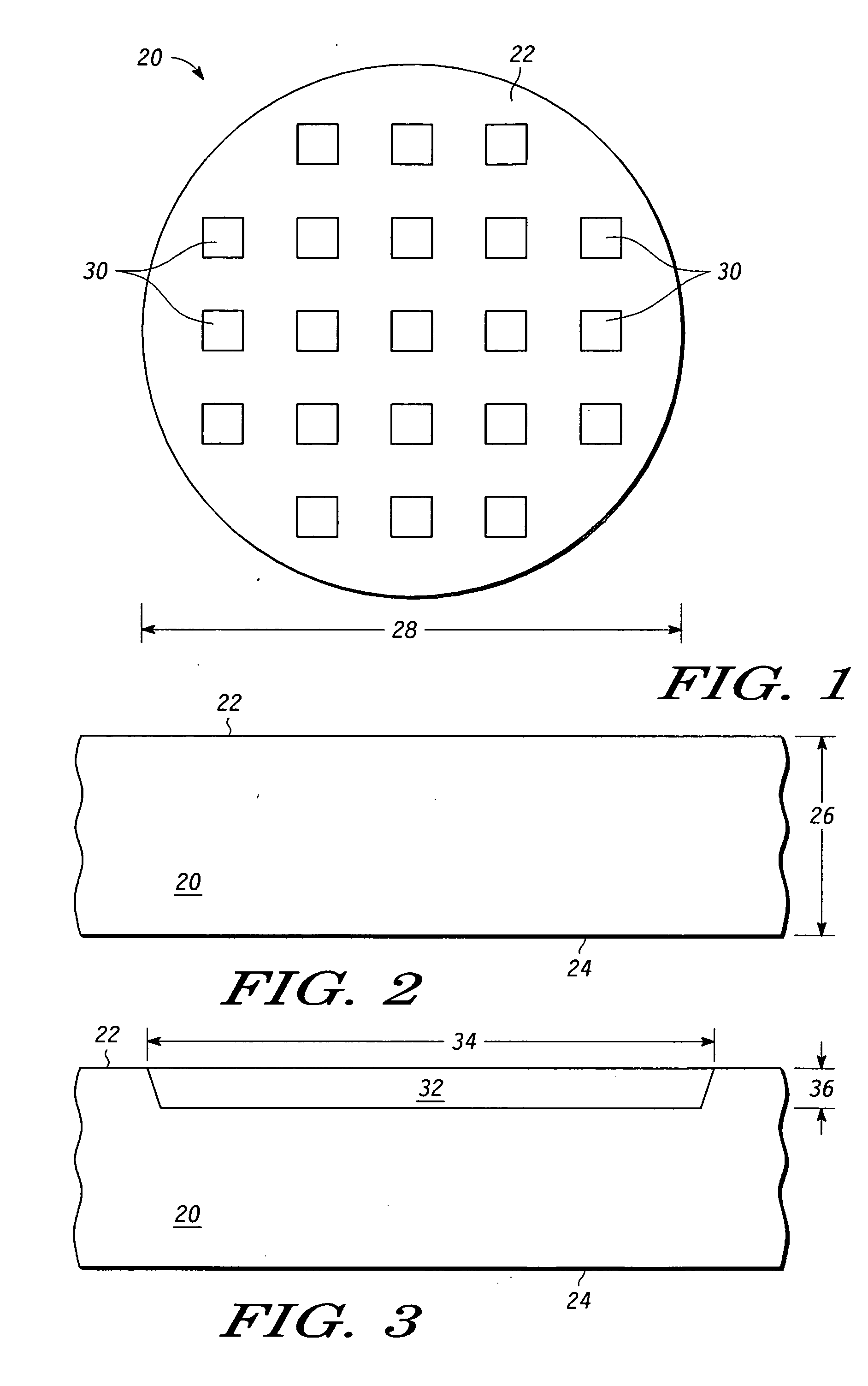
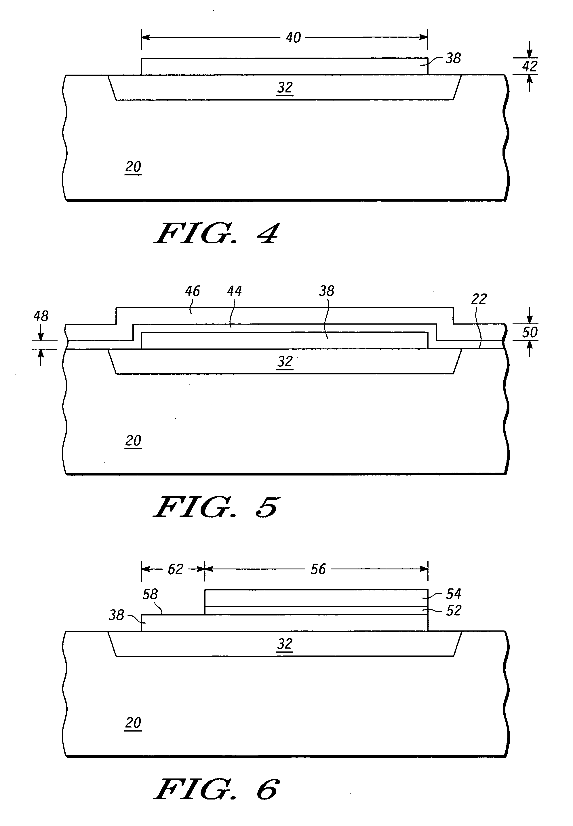
[0019] The following detailed description is merely exemplary in nature and is not intended to limit the invention or application and uses of the invention. Furthermore, there is no intention to be bound by any expressed or implied theory presented in the preceding technical field, background, brief summary, or the following detailed description. It should also be noted that FIGS. 1-11 are merely illustrative and may not be drawn to scale.

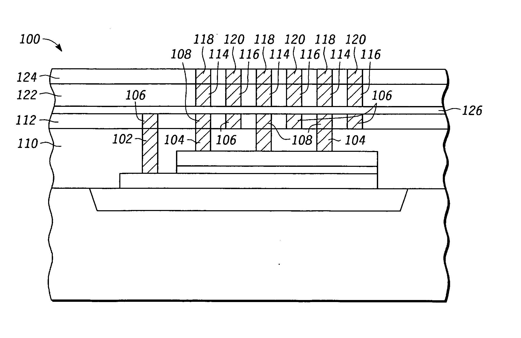
[0020]FIG. 1 to FIG. 9 illustrate a method for forming an electronic (or microelectronic) assembly, or a semiconductor device, according to one embodiment of the present invention. A capacitor having first and second conductors is formed on a semiconductor substrate. A build up layer is then formed over the capacitor. The build up layer includes first and second sets of conductive members, such as conductive traces. The first and second sets of conductive members form interdigitated “combs” to maximize the fringe capacitance therebetween and form ...


PUM


Abstract

An electronic assembly (98) includes a substrate (20), a capacitor having first and second conductors (38,54) formed over the substrate, a first set of conductive members (76) formed over the substrate and being electrically connected to the first conductor of the capacitor, and a second set of conductive members (78) formed over the substrate and being electrically connected to the second conductor of the capacitor.

Description

FIELD OF THE INVENTION [0001] The present invention generally relates to a microelectronic assembly and a method for forming a microelectronic assembly, and more particularly relates to a composite capacitor and a method for forming the same. BACKGROUND OF THE INVENTION [0002] In recent years, semiconductor integrated circuits have become more complicated both in terms of packing density and the variety of device components that are included in a single circuit. As the productivity and performance demands increase, the size of integrated circuits, and the microelectronic dies (or “dice”), or semiconductor chips, on which they are formed continues to be reduced. As the devices become smaller and smaller, it is increasingly difficult to find room on each die for all of the desired components. Passive device components, particularly capacitors, can be greatly affected as the performance of such devices is often dependent on the surface area of die used. [0003] Depending on the intended...

Claims


Application Information

Patent Timeline
Patent Type & Authority Applications(United States)
IPC IPC(8): H01L29/00H01G4/30
CPCH01G4/236H01G4/33H01L28/60H01L27/0805H01L23/5223H01L2924/0002H01L2924/00
Inventor MIN, WON GIFALLICO, GENO L.KROLL, AMANDA M.YANG, HONGNINGZUO, JIANG-KAI
Owner NXP USA INC
Why Eureka
Try Eureka