
Nonvolatile Semiconductor Memory

a semiconductor memory and non-volatile technology, applied in semiconductor devices, digital storage, instruments, etc., can solve the problems of difficult to realize gate lengths of 130 nm for memory cells of nor type flash memory, and achieve the effect of reducing the potential difference, reducing the number of voltage stepping-up circuits to generate the voltage in the chip, and scaling the chip area

Inactive Publication Date: 2007-10-04
GENUSION
View PDF5 Cites 17 Cited by
  • Summary
  • Abstract
  • Description
  • Claims
  • Application Information

AI Technical Summary

Benefits of technology

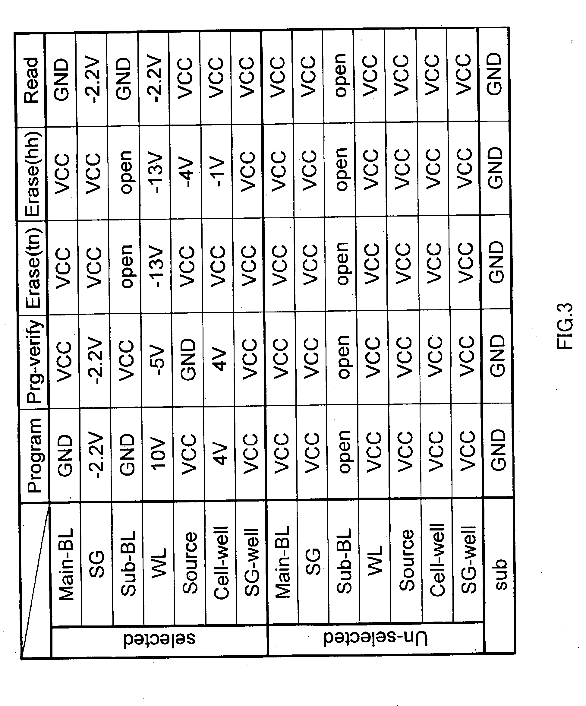
[0036] According to the present invention, setting the voltages in a relationship of “Vg>Vsub>Vs>Vd (p-channel)” or “Vg<Vsub<Vs<Vd (n-channel)”, i.e., setting the source voltage Vs between the cell well voltage Vsub and the drain voltage Vd, causes hot electrons or hot holes to be generated efficiently by band to band tunneling, minimizes the potential difference between the source and the drain, and therefore scales the gate length. For fast writing, the potential difference of the cell well voltage Vsub and the drain voltage Vd is preferred to be equivalent or not less than the barrier voltage of the tunneling insulating layer.
[0037] Furthermore, according to the present invention, the number of voltage stepping-up circuits to generate the voltages in a chip can be reduced by supplying any one of the voltages Vg, Vsub, Vs and Vd from the external power supply. Therefore, a chip area can be scaled and the cost of a nonvolatile semiconductor memory device can be reduced.
[0038] Particularly, supplying the drain voltage Vd, which consumes the largest amount of current during writing, from an external power supply, may reduce the capability to supply the current of the voltage stepping-up circuits in the chip, and a chip area can be further scaled.
[0039] Furthermore, according to the present invention, by applying an appropriate back gate voltage to the cell well, the source voltage Vs can be the power supply voltage and the drain voltage Vd can be the ground voltage, and allows two of the four voltages to be supplied from the external supply and allows the remaining two voltages (the gate voltage Vg, the cell well voltage Vsub) to be voltages with the same polarity to the power supply voltage.

Problems solved by technology

According to the technology prediction by ITRS (International Technology Roadmap for Semiconductors) in 2004, even in 2018 when 20 nm semiconductor process technology is predicted to be utilized, it is said to be difficult to realize gate lengths of 130 nm for memory cells of a NOR type flash memory.

Method used


Image

  • Nonvolatile Semiconductor Memory
  • Nonvolatile Semiconductor Memory
  • Nonvolatile Semiconductor Memory

Examples


Embodiment Construction

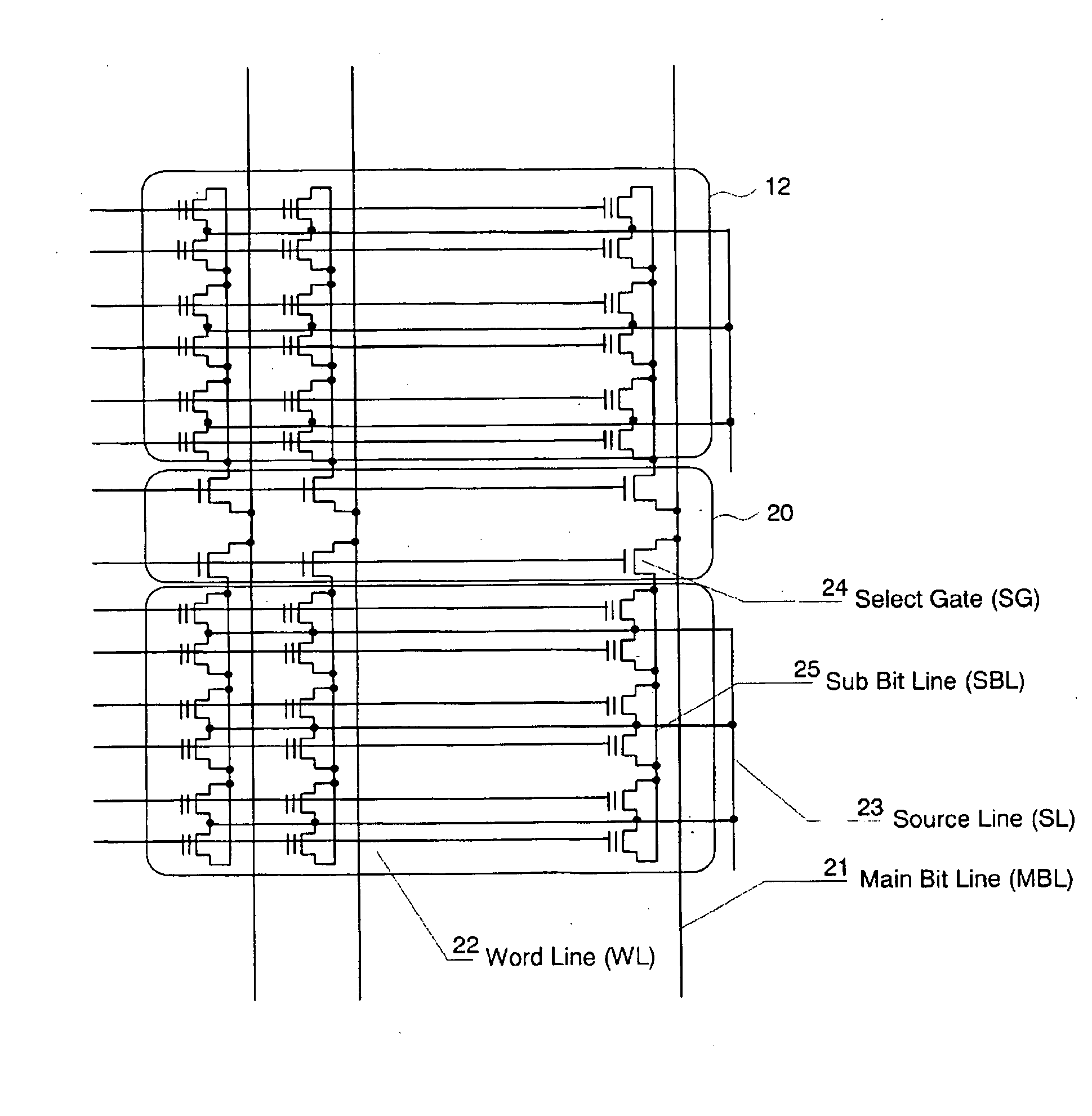
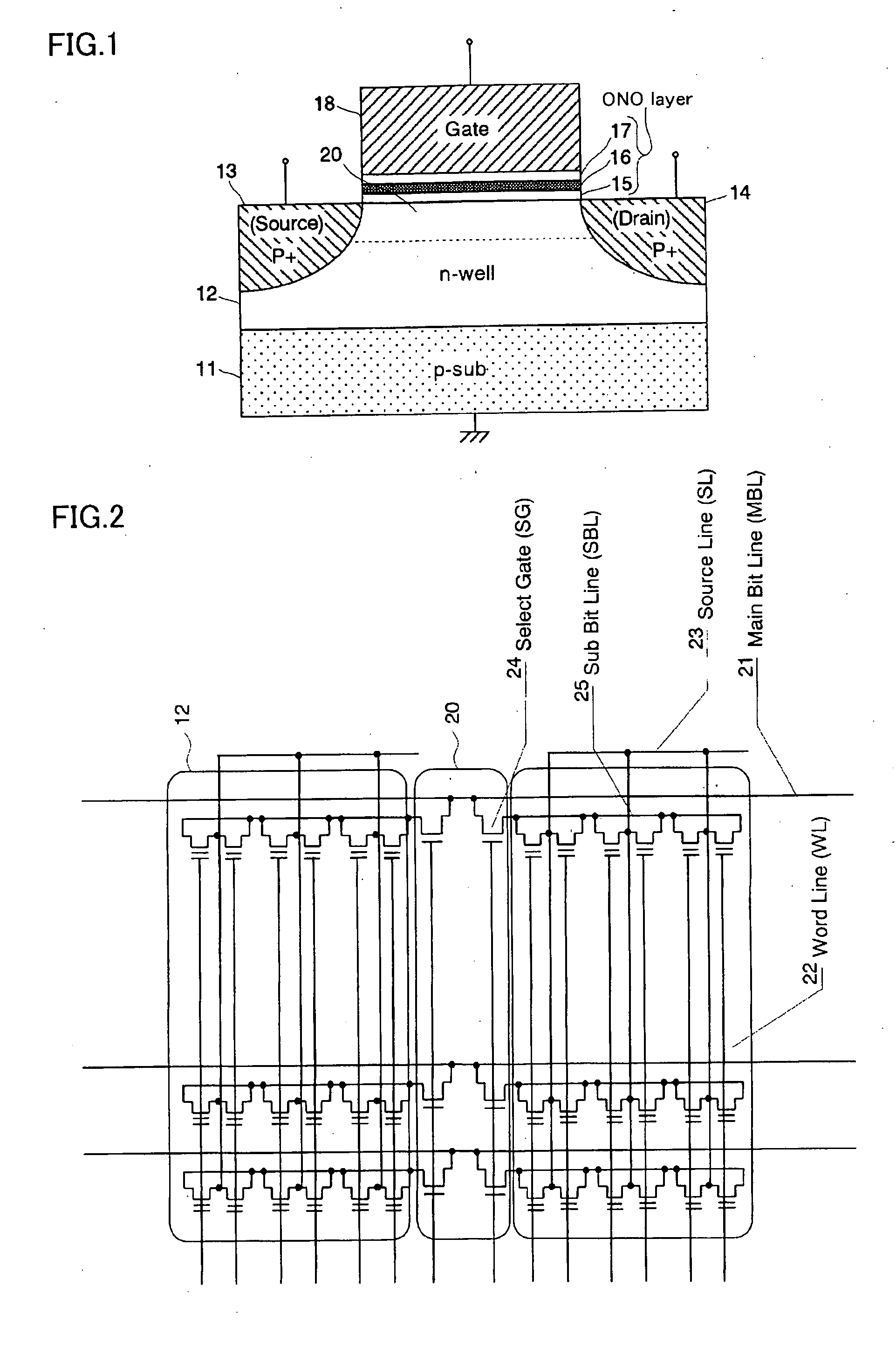
[0086] The embodiments of the invention will be explained with reference to the accompanying drawings. FIG. 1 shows a schematic configuration of the p-channel MONOS memory cell implementing the present invention. The memory cell has an n type well (cell well) 12 formed in a semiconductor substrate 11, a p+ region (source) 13 and a p+ region (drain) 14 formed near the surface of the n type well with a predetermined interval, a channel region 20 formed between the two p type regions 13 and 14, and an ONO layer and a gate electrode 18 formed above the channel region 20 and to cover the channel region 20.

[0087] The ONO layer consists of a tunnel insulating layer 15 made by silicon oxide, a charge trap layer 16 to accumulate injected charges made by silicon nitride and an insulating layer 17 made by silicon oxide. The thicknesses of these three layers: the thickness of the tunnel insulating layer 15 is approximately 2.5˜5 nm, the thickness of the charge trap layer 16 is approximately 10...


PUM


Abstract

A hot electron (BBHE) is generated close to a drain by tunneling between bands, and it data writing is performed by injecting the hot electron into a charge storage layer. When Vg is a gate voltage, Vsub is a cell well voltage, Vs is a source voltage and Vd is a drain voltage, a relation of Vg>Vsub>Vs>Vd is satisfied, Vg−Vd is a value of a potential difference required for generating a tunnel current between the bands or higher, and Vsub−Vd is substantially equivalent to a barrier potential of the tunnel insulating film or higher.

Description

RELATED APPLICATIONS [0001] This application is a continuation in part of and claims the benefit of priority to U.S. patent application Ser. No. 10 / 598,853 filed on Sep. 13, 2006, which claims the benefit of priority to PCT Application PCT / JP2005 / 020063 filed on Nov. 1, 2005.TECHNICAL FIELD [0002] The present invention relates to a nonvolatile semiconductor storage device which realizes scaling of gate lengths of nonvolatile semiconductor memory cells, and method for writing therein. BACKGROUND OF THE INVENTION [0003] Recently, concern over the limit of scaling of a NOR type flash memory for code storage having a capability of random access, is increasing. [0004] According to the technology prediction by ITRS (International Technology Roadmap for Semiconductors) in 2004, even in 2018 when 20 nm semiconductor process technology is predicted to be utilized, it is said to be difficult to realize gate lengths of 130 nm for memory cells of a NOR type flash memory. [0005] One of the main ...

Claims


Application Information

Patent Timeline
Patent Type & Authority Applications(United States)
IPC IPC(8): G11C16/10
CPCG11C11/5671G11C16/0466G11C16/08H01L27/11568H01L27/105H01L27/115H01L27/11524G11C16/12H10B41/35H10B43/30H10B69/00
Inventor AJIKA, NATSUOSHUKURI, SHOJIMIHARA, MASAAKINAKASHIMA, MORIYOSHI
Owner GENUSION
Learn More