
Cleaning Agent for Substrate and Cleaning Method

Inactive Publication Date: 2007-10-11
WAKO PURE CHEMICAL INDUSTRIES
View PDF7 Cites 49 Cited by
  • Summary
  • Abstract
  • Description
  • Claims
  • Application Information

AI Technical Summary

Benefits of technology

[0013] The present invention has been made under such circumstances as described above, and provides a cleaning agent for a substrate and a cleaning method thereof, which can effectively remove fine particles (particles) present on a surface of substrate or impurities (metallic impurities) derived from various kinds of metals, without causing roughness surface of a substrate, in particular, a semiconductor substrate, and without causing corrosion or oxidation of metal wirings, in particular, copper wirings, provided on a surface of substrate, and further can remove at the same time the carbon defect present on a surface of substrate, without removing a metal corrosion inhibitor—Cu film, in particular, a Cu-BTA film. MEANS TO SOLVE THE PROBLEMS
[0017] Namely, the present inventors have, after intensively studying a way to achieve the above-described object, found that not only particles and metallic impurities on a surface of substrate can be removed without causing roughness surface of a semiconductor substrate or corrosion or oxidation of metal wirings, in particular, cupper wirings provided on a semiconductor substrate, but also a carbon defect remaining on a substrate surface can also be easily removed at the same time without losing a metal corrosion inhibitor—Cu film, in particular, a Cu-BTA film, by cleaning the substrate surface using a cleaning agent for substrate comprising [I] an organic acid having at least one carboxyl group and / or [II] a complexing agent and [III] a specified organic solvent, in particular, a cleaning agent for substrate comprising [I] an organic acid having at least one carboxyl group, [II] a complexing agent and [III] a specified organic solvent, and further that specified solvents, among organic solvents, are superior in exhibiting such an effect, and a combined use of the specified organic solvents and a compound having at least one phosphonic acid group in a molecule (a phosphonic acid type complexing agent) as a complexing agent is particularly preferable, and accomplished the present invention.
[0028] The organic solvent according to the present invention can remove a carbon defect without removing a metal corrosion inhibiting film (for example, a metal corrosion inhibitor—Cu film such as a Cu-BTA film) which has been formed on a surface of semiconductor substrate, and also can remove a carbon defect without dissolving, corroding, oxidizing or decomposing apparatus components relating to device production such as semiconductor materials, wiring materials and plug materials.

Problems solved by technology

And the semiconductor surface after the CMP process is contaminated with a large amount of abrasive grain itself used, metals contained in the slurry, or metallic impurities derived from metallic wirings or metallic plug polished, and further various kinds of particles.
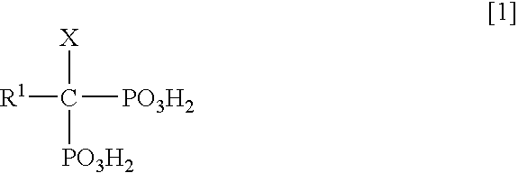
Contamination of the surface of semiconductor substrate with the metallic impurities or the particles affects electric characteristics of the semiconductor, and causes to lose reliability of devices.
Further, since device is destructed when metallic contamination is significant, it is necessary to introduce a post-CMP cleaning process to remove metallic impurities or particles from the surface of semiconductor substrate.
On the other hand, since metallic copper on a surface of semiconductor is highly active, and easily corroded by a slight oxidizing power, it tends to cause an increase of wiring resistance or wire breaking.
However, these metal corrosion inhibitors may remain on a surface of semiconductor as a so-called carbon defect.
There has been a problem that when a semiconductor having a carbon defect remaining on a surface thereof is subjected to heat treatment in the subsequent process, during working of a device or the like, the carbon defect is burnt to oxidize a wiring material resulting in deterioration of the device performance, or an apprehension that multilayer wiring executed without removing the carbon defect tends to put the flatness of upper layer part into disorder, and make a correct lamination difficult to cause a serious defect in working of the device.
However, a cleaning agent, which is conventionally used in various cleaning processes such as a post-CMP cleaning process, cannot sufficiently remove the carbon defect, or apt to remove a metal corrosion inhibiting film that is needed to prevent corrosion of metal surface as described above.
Thus, an effective means has not been found which can remove only the carbon defect while maintaining the metal corrosion inhibiting effect, without removing a metal corrosion inhibitor—Cu film, in particular, a Cu-BTA film as described above.

Method used


Image

  • Cleaning Agent for Substrate and Cleaning Method
  • Cleaning Agent for Substrate and Cleaning Method
  • Cleaning Agent for Substrate and Cleaning Method

Examples


examples 1 to 44

[0110] Each of the wafer contaminated with a carbon defect, the wafer provided with a Cu-BTA film and the metallic Cu deposited wafer, which were prepared by the above-described methods, was dipping in 1 L of each cleaning agent described in Table 1 at room temperature for 5 hours. Thereafter, each of waters was taken out, rinsed with ultra pure water for 10 min, and spin-dried.

[0111] As to the wafer contaminated with a carbon defect thus treated, presence of the carbon defect adsorbed and remaining on said wafer surface was confirmed to evaluate capability of removing carbon defect, by direct measurement using an Auger photoelectron spectroscopic analyzer.

[0112] And as to the wafer provided with a Cu-BTA film, thickness of a Cu-BTA film on the wafer surface was measured to confirm an influence (occurrence of dissolution and elution) on the Cu-BTA film.

[0113] Further, as to the metallic Cu deposited wafer, color tone of a Cu film surface on the wafer surface was checked by visual...

examples 45 to 76

[0122] Each of the wafers contaminated with metals prepared by the above-described method was dipped in 1 L each of cleaning agents described in Table 4, at room temperature for 1 hour. Thereafter, the wafer was taken out, rinsed with ultra pure water for 10 min, and spin-dried.

[0123] For the wafers contaminated with metals thus treated, remaining metal concentrations (remaining Fe concentration, remaining Al concentration, and remaining Cu concentration) adsorbed and remaining on a surface of the wafer were measured, to evaluate capability of removing metallic impurities.

[0124] The results are shown in Table 4.

TABLE 4remainingremainingremainingconc.Complex-conc.conc.Fe conc.Al conc.Cu conc.Ex.Organic acid(% by WT)ing agent(% by WT)Organic solvent(% by WT)pH(Fe atom / cm2)(Al atom / cm2)(Cu atom / cm2)45citric acid5—methanol0.224 × 10139 × 10122 × 101246acetic acid5—methanol0.226 × 10124 × 10124 × 101247malonic acid5—isopropylalcohol537 × 10128 × 10123 × 101248fumaric acid5—2-methoxye...

examples 77 to 108

[0129] The wafers contaminated with metals prepared by the above method were subjected to a brush scrub cleaning using a brush made of poly(vinyl alcohol), while each of the cleaning agents described in Table 6 was sprayed on a surface of said wafers. The treatment temperature was 25° C., and cleaning time was 1 min. After cleaning, the wafers were rinsed with ultra pure water for 10 min, and spin-dried.

[0130] For the wafers contaminated with metals thus treated, remaining metal concentrations (remaining Fe concentration, remaining Al concentration, and remaining Cu concentration) adsorbed and remaining on a surface of the wafer were measured, to evaluate capability of removing metallic impurities.

[0131] The results are shown in Table 6

TABLE 6conc.remainingremainingremaining(% byComplexingconc.conc.Fe conc.Al conc.Cu conc.Ex.Organic acidWT)agent(% by WT)Organic solvent(% by WT)pH(Fe atom / cm2)(Al atom / cm2)(Cu atom / cm2)77citric acid5—methanol0.228 × 10121 × 10131 × 101378acetic aci...


PUM

PropertyMeasurementUnit
Metallic bondaaaaaaaaaa
Semiconductor propertiesaaaaaaaaaa

Abstract

The present invention provides a cleaning agent for a substrate and a cleaning method thereof, which can effectively remove fine particles (particles) present on a surface of substrate or impurities derived from various kinds of metals (metallic impurities), without causing roughness surface of a substrate, in particular, a semiconductor substrate, and without causing corrosion or oxidation of metal wirings, in particular, copper wirings, provided on a surface of substrate, and can further remove at the same time a carbon defect present on a surface of substrate, without removing a metal corrosion inhibitor—Cu film, in particular, a Cu-BTA film. The present invention provides a cleaning agent for a substrate comprising [I] an organic acid having at least one carboxyl group and / or [II] a complexing agent, and [III] an organic solvent selected from the group consisting of (1) monohydric alcohols, (2) alkoxyalcohols, (3) glycols, (4) glycol ethers, (5) ketones and (6) nitriles, and a cleaning method for a surface of substrate, which comprises the surface of substrate is treated with said cleaning agent.

Description

TECHNICAL FIELD [0001] The present invention relates to a cleaning agent for a surface of substrate, in particular, for a surface of semiconductor substrate provided with copper wiring thereon, and to a cleaning method thereof. BACKGROUND ART [0002] Recently, with the spread of multilayer wirings on a surface of semiconductor substrate, a so-called chemical mechanical polishing (CMP) technique, by which a semiconductor substrate is mechanically polished and planarized, has been used in producing devices. [0003] In particular, accompanied to the tendency to a highly integrated LSI in recent years, a wiring used has been changed from conventional aluminum to copper (Cu) which has a lower electric resistance, and thus the CMP technique (Cu-CMP) has become essential, when semiconductors having a multilayer structure, in which copper wirings are provided in many layers on the surface thereof, are produced. [0004] The CMP is a method for planarizing a surface of semiconductor substrate us...

Claims


Application Information

Patent Timeline
IPC IPC(8): C11D1/68C11D7/26C11D7/32C11D7/36C11D11/00C23G5/02C23G5/032H01L21/306
CPCC11D7/261C11D7/262C11D7/263C11D7/264H01L21/02052C11D7/36C11D11/0047C23G5/02C23G5/032C11D7/3245C11D2111/22C11D7/32C11D11/00
Inventor MIZUTA, HIRONORIKAKIZAWA, MASAHIKOHAYASHIDA, ICHIRO
Owner WAKO PURE CHEMICAL INDUSTRIES
Learn More