
Capacitor device having three-dimensional structure

a capacitor and three-dimensional technology, applied in the field of capacitor devices, can solve the problems of capacitor devices having three-dimensional structures, capacitor devices that cannot be reliably enhanced, capacitor devices with capacitor devices that have capacitor devices that cannot be expected to be polarized to increase, etc., to achieve the effect of preventing deterioration of capacitor devices, effective application of tensile stress, and high moisture conten

Inactive Publication Date: 2007-10-11
PANASONIC CORP
View PDF4 Cites 10 Cited by
  • Summary
  • Abstract
  • Description
  • Claims
  • Application Information

AI Technical Summary

Benefits of technology

[0013] The present invention has been made to solve the aforementioned conventional problems, and an object of the present invention is to provide a high-reliability capacitor device having a three-dimensional structure while increasing the polarization of the capacitor device by applying a tensile stress to a ferroelectric film and preventing deterioration in the capacitor device due to moisture.
[0016] According to the capacitor device of the present invention, an insulating film having a high moisture content and causing tensile stress can be formed on the stress control layer. This permits effective application of a tensile stress to the ferroelectric film and can prevent deterioration in the capacitor device due to moisture. As a result, a high-reliability capacitor device having a three-dimensional structure can be achieved.
[0017] In the capacitor device of the present invention, the stress control layer preferably functions as a hydrogen diffusion barrier. This structure can prevent the capacitor device from being deteriorated due to entry of hydrogen into the ferroelectric film.
[0018] In the capacitor device of the present invention, the stress control layer is preferably a single layer made of any one of titanium nitride, titanium aluminum nitride, titanium aluminum oxide, tantalum aluminum nitride, tantalum aluminum oxide, and tantalum silicon nitride or a multilayer made of at least two thereof. With this structure, a stress control layer causing tensile stress and functioning as a moisture diffusion barrier can be formed with reliability.
[0021] It is preferable that the capacitor device of the present invention further includes a second interlayer insulating film formed between the upper electrode and the stress control layer and causing tensile stress. With this structure, the vertical dimension of the upper electrode can be reduced, and a stress control layer can be formed with reliability. In this case, the second interlayer insulating film is preferably a silicon oxide film formed by thermal chemical vapor deposition using ozone and tetraethoxysilane as its materials and subjected to heat treatment.

Problems solved by technology

As a result, the polarization of the capacitor device cannot be expected to increase, and thus the possibility of causing semiconductor memory devices having capacitor devices to malfunction is increased.
In other words, when a film causing compressive stress is used as an interlayer insulating film, the reliability of capacitor devices having a three-dimensional structure and using a ferroelectric material for a capacitor insulating film cannot be enhanced.

Method used


Image

  • Capacitor device having three-dimensional structure
  • Capacitor device having three-dimensional structure
  • Capacitor device having three-dimensional structure

Examples


embodiment 2

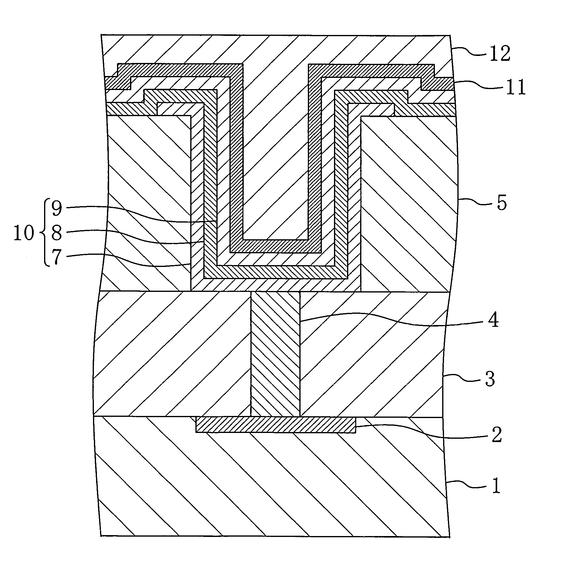
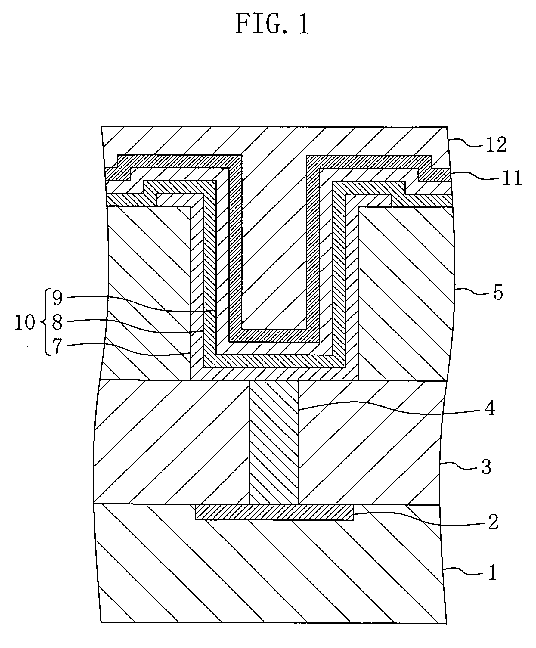
[0058] A capacitor device according to a second embodiment of the present invention will be described with reference to the drawings. FIG. 6 illustrates a cross-sectional shape of the capacitor device according to the second embodiment. In FIG. 6, the same components as those in FIG. 1 are identified by the same reference numerals and description will not be given to them.

[0059] As illustrated in FIG. 6, a fourth interlayer insulating film 31 causing tensile stress is formed between an upper electrode 9 and a stress control layer 11.

[0060] The formation of the fourth interlayer insulating film 31 can improve the step coverage of the stress control layer 11. In general, the stress control layer 11 is formed of metal nitride or metal oxide and therefore formed by sputtering. However, it is difficult to form a film completely covering the corners of the capacitor element in the use of sputtering. The formation of the fourth interlayer insulating film 31 reduces the vertical dimension...


PUM


Abstract

A capacitor device having a three-dimensional structure includes: a lower electrode formed on a semiconductor substrate to have a three-dimensional shape; a capacitor insulating film formed to cover the lower electrode and made of a ferroelectric material; and an upper electrode formed on the capacitor insulating film to have a step portion. A stress control layer is formed on the upper electrode to cause tensile stress and function as a moisture diffusion barrier.

Description

CROSS-REFERENCE TO RELATED APPLICATIONS [0001] This application claims priority under 35 U.S.C. §119 on Patent Application No. 2005-163965 filed in Japan on Jun. 3, 2005, the entire contents of which are hereby incorporated by reference. BACKGROUND OF THE INVENTION [0002] (1) Field of the Invention [0003] The present invention relates to capacitor devices using a ferroelectric material as a capacitor insulating film and having a three-dimensional structure. [0004] (2) Description of Related Art [0005] To commercialize a RAM which enables high-speed writing and reading at an unprecedentedly low voltage, vigorous research and development has been made on capacitor devices made of a ferroelectric material having a characteristic of spontaneous polarization. To implement a megabit-class semiconductor memory device to be mounted on an LSI composed of a complementary metal oxide semiconductor (CMOS) with design rules of 0.18 μm or below, in particular, a capacitor device having a three-di...

Claims


Application Information

Patent Timeline
IPC IPC(8): H01L27/108
CPCH01L27/11502H01L28/55H01L27/11507H10B53/30H10B53/00
Inventor NAGANO, YOSHIHISAJUDAI, YUJI
Owner PANASONIC CORP
Learn More