Method for Manufacturing Simox Wafer and Simox Wafer Obtained by This Method

a manufacturing method and technology of simox wafer, applied in semiconductor/solid-state device manufacturing, basic electric elements, electric apparatus, etc., can solve the problems of rough surface of soi layer and rough interface between, particle size measurable on the surface of silicon wafer cannot be measured on the surface of simox wafer,

Inactive Publication Date: 2007-10-11
SUMCO CORP
View PDF20 Cites 8 Cited by
  • Summary
  • Abstract
  • Description
  • Claims
  • Application Information

AI Technical Summary

Benefits of technology

[0031]As described above, according to the method for manufacturing the present invention, when the first dose amount in the process of forming the first ion-implanted layer is set to 2×10¹⁷ to 3×10¹⁷ atoms/cm2, the first implantation energy is set to 165 to 240 keV and the second dose amount in the step of forming the second ion-i

Problems solved by technology

However, in the SIMOX wafer obtained by the manufacturing method described in U.S. Patent Publication Specification No. 5930643, roughness of a surface of the SOI layer and roughness of the interface between the SOI layer and the BO

Method used


Image

  • Method for Manufacturing Simox Wafer and Simox Wafer Obtained by This Method
  • Method for Manufacturing Simox Wafer and Simox Wafer Obtained by This Method
  • Method for Manufacturing Simox Wafer and Simox Wafer Obtained by This Method

Examples


examples

[0070]Next, an example of the present invention will be described in detail with a comparative example.

examples 1-1 through 1-6

, Comparative examples 1-1 and 1-2

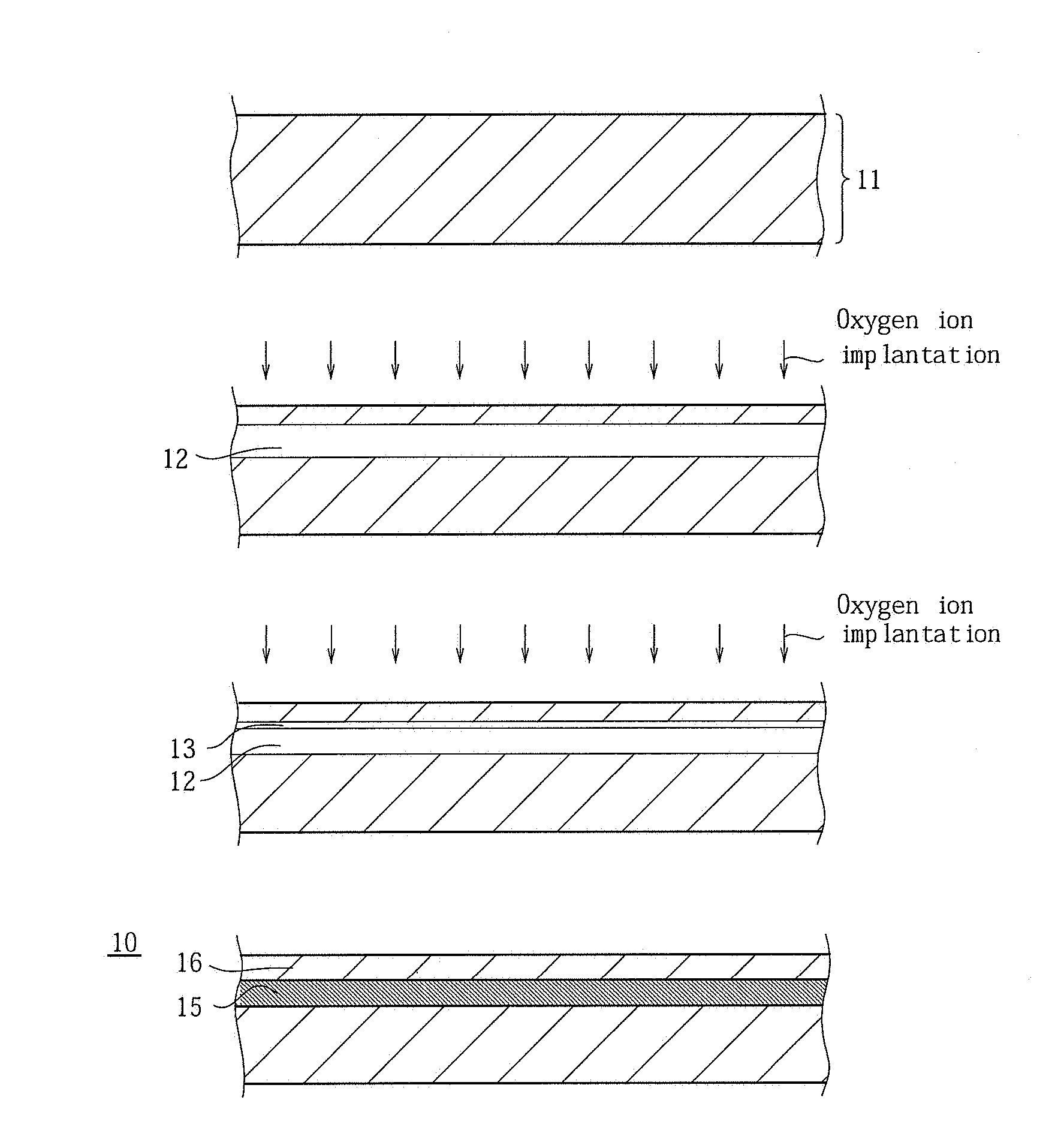
[0071]As shown in FIG. 1, there was prepared a silicon wafer 11 which is a P-type silicon wafer of which diameter is 300 mm, crystal orientation is , and resistivity is 10 to 20 ohm-cm. Firstly, after accommodating the wafer 11 in the ion implanter, the inside of the apparatus was made a vacuum state and the temperature inside the apparatus was heated to 400° C.

[0072]Next, ion implantation of oxygen ions (O+) was performed in a first dose amount of 2.5×10¹⁷ atoms / cm2 with a first implantation energy from the surface of the wafer 11, and a first ion-implanted layer 12 having a peak at the first depth of 0.4 to 0.5 micrometers from the surface of the wafer 11 was formed. Thereafter, the temperature inside the apparatus was cooled down to a room temperature.

[0073]Next, the wafer 11 was taken out from the apparatus to be cleaned. After drying the cleaned wafer 11, it was accommodated into the apparatus again. Subsequently, ion implantation of oxygen ion...

examples 2-1 through 2-4

[0077]There was obtained a SIMOX wafer 10 in a manner similar to that of Examples 1-1 through 1-6 and Comparative examples 1-1 and 1-2 except that ion implantation was changed from a single implantation step to double implantation steps in the process of forming the first ion-implanted layer, oxygen ions (O+) in the first step was set to 1.25×10¹⁷ atoms / cm2 and oxygen ions (O+) in the second step was set to 1.25×10¹⁷ atoms / cm2, the averages of first implantation energy of the first step and the second step were set to 172 keV, 176 keV, 180 keV, and 184 keV, respectively, and the value obtained by deducting the first implantation energy of the second step from the first implantation energy of the first step was set to 8 keV. The SIMOX wafers 10 obtained by the above-mentioned methods are referred to as Examples 2-1 through 2-4, respectively.


PUM


Abstract

It is an object of the present invention to provide a method for manufacturing SIMOX wafer, wherein roughness Rms of a measurement area of 10 square micrometers in a surface of an SOI layer and roughness Rms of a measurement area of 10 square micrometers in an interface between the SOI layer and a BOX layer can be reduced respectively and a SIMOX obtained by the method. The method is to manufacture a SIMOX wafer comprising; a step of forming a first ion-implanted layer 12 containing highly concentrated oxygen within a wafer 11; a step of forming a second ion-implanted amorphous layer 13; and a high temperature heat treatment step of transforming the first and second ion-implanted layers into a BOX layer 15 by holding the wafer at a temperature between 1300° C. or more and a temperature less than a silicon melting point in an atmosphere containing oxygen, wherein when a first dose amount in the step of forming the first ion-implanted layer is set to 2×10¹⁷ to 3×10¹⁷ atoms/cm2, the first implantation energy is set to 165 to 240 keV and a second dose amount in the step of forming the second ion-implanted layer is set to 1×10¹⁴ to 1×10¹⁶ atoms/cm2.

Description

BACKGROUND OF THE INVENTION[0001]1. Field of the Invention[0002]The present invention relates to a method for manufacturing a SIMOX wafer based on a SIMOX (Separation by IMplanted OXygen) technology among methods for manufacturing an SOI (Silicon On Insulater) wafer in which a single crystal silicon layer is formed in a silicon single crystal main body via an oxide film and a SIMOX wafer obtained by use of the method.[0003]2. Description of the Related Art[0004]Conventionally, two methods have been known as a method for manufacturing an SOI wafer, one is a bonding method in which two wafers are bonded with each other via an oxide film, and the other is a SIMOX method in which oxygen ions (O+) are implanted from a surface of the silicon wafer to form an ion-implanted layer of a single crystal containing highly concentrated oxygen in a region of a predetermined depth within the wafer, and then this wafer is subjected to a heat treatment to thereby transform the ion-implanted layer int...

Claims


Application Information

Patent Timeline
IPC IPC(8): H01L21/20
CPCH01L21/76243H01L21/26533H01L21/02H01L21/20
Inventor AOKI, YOSHIROKASAMATSU, RIYUUSUKEKOMATSU, YUKIO
Owner SUMCO CORP
Why Eureka
Try Eureka