Phase change memory element with a peripheral connection to a thin film electrode and method of manufacture thereof

a memory element and peripheral connection technology, applied in the field of memory devices, can solve the problems of reducing the crystallization speed of germanium-antimony-tellurium material with thinner films, the practicality of memory devices in producing and controlling dimensions well below the norms, and the current applied during the reset pulse may actually set the material in some cells, etc., to achieve good performance, small cross-sectional area, and high current density

Inactive Publication Date: 2007-11-01
IBM CORP
View PDF8 Cites 79 Cited by
  • Summary
  • Abstract
  • Description
  • Claims
  • Application Information

AI Technical Summary

Benefits of technology

[0027] Because effective heating of the phase change material requires only a high current density, reducing the contact area between the phase change material and one of the electrodes is sufficient to manage the power requirements. Thus, for example, good performance can be obtained from a long, narro

Problems solved by technology

However, the crystallization speed of a germanium-antimony-tellurium material tends to decrease with thinner films.
If the dimensions vary excessively, on an all-cells/all-die/all-days basis, there is a risk that the current applied during the Reset pulse may actually set the material in some cells, and vice-versa

Method used


Image

  • Phase change memory element with a peripheral connection to a thin film electrode and method of manufacture thereof
  • Phase change memory element with a peripheral connection to a thin film electrode and method of manufacture thereof
  • Phase change memory element with a peripheral connection to a thin film electrode and method of manufacture thereof

Examples


Embodiment Construction

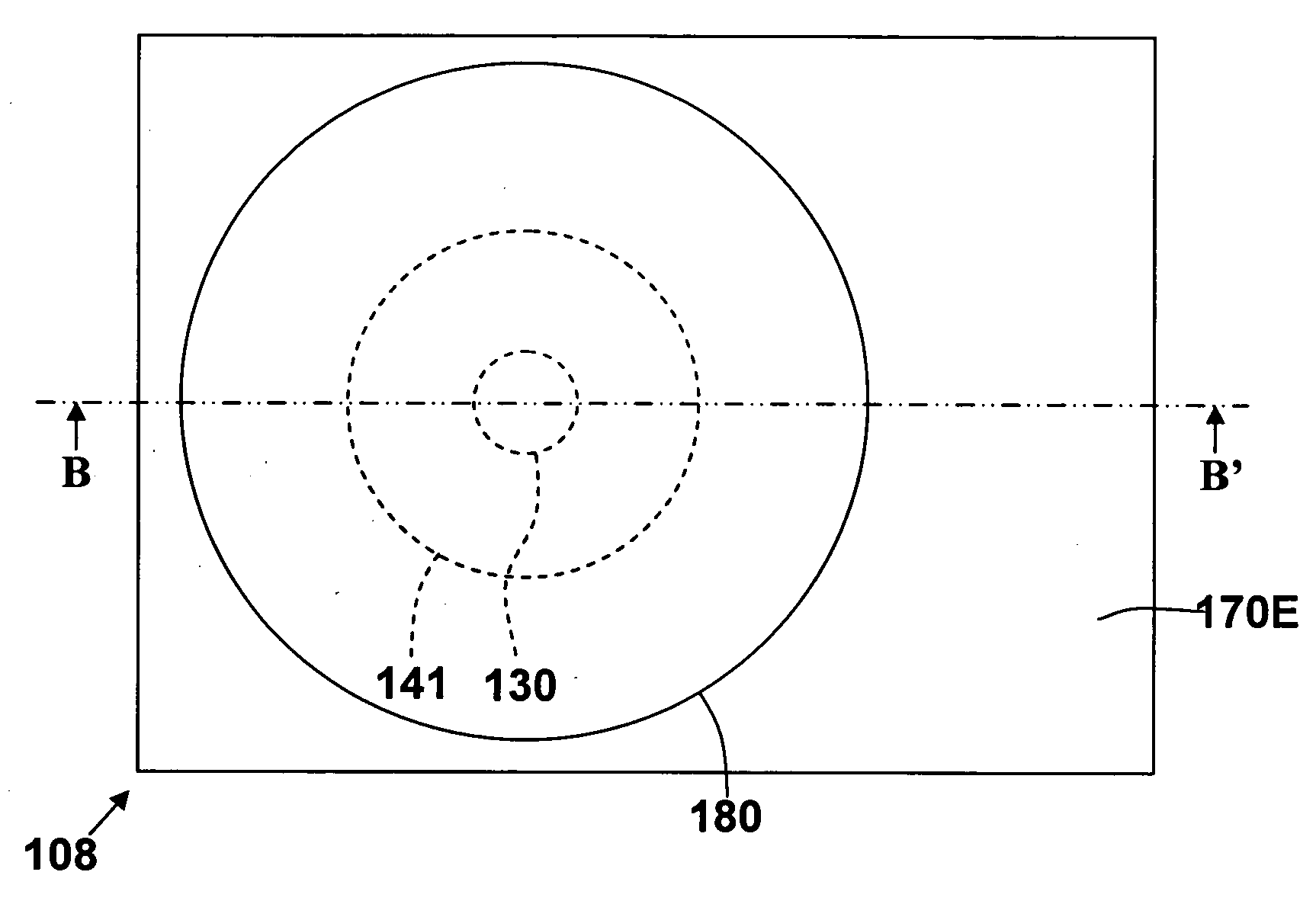
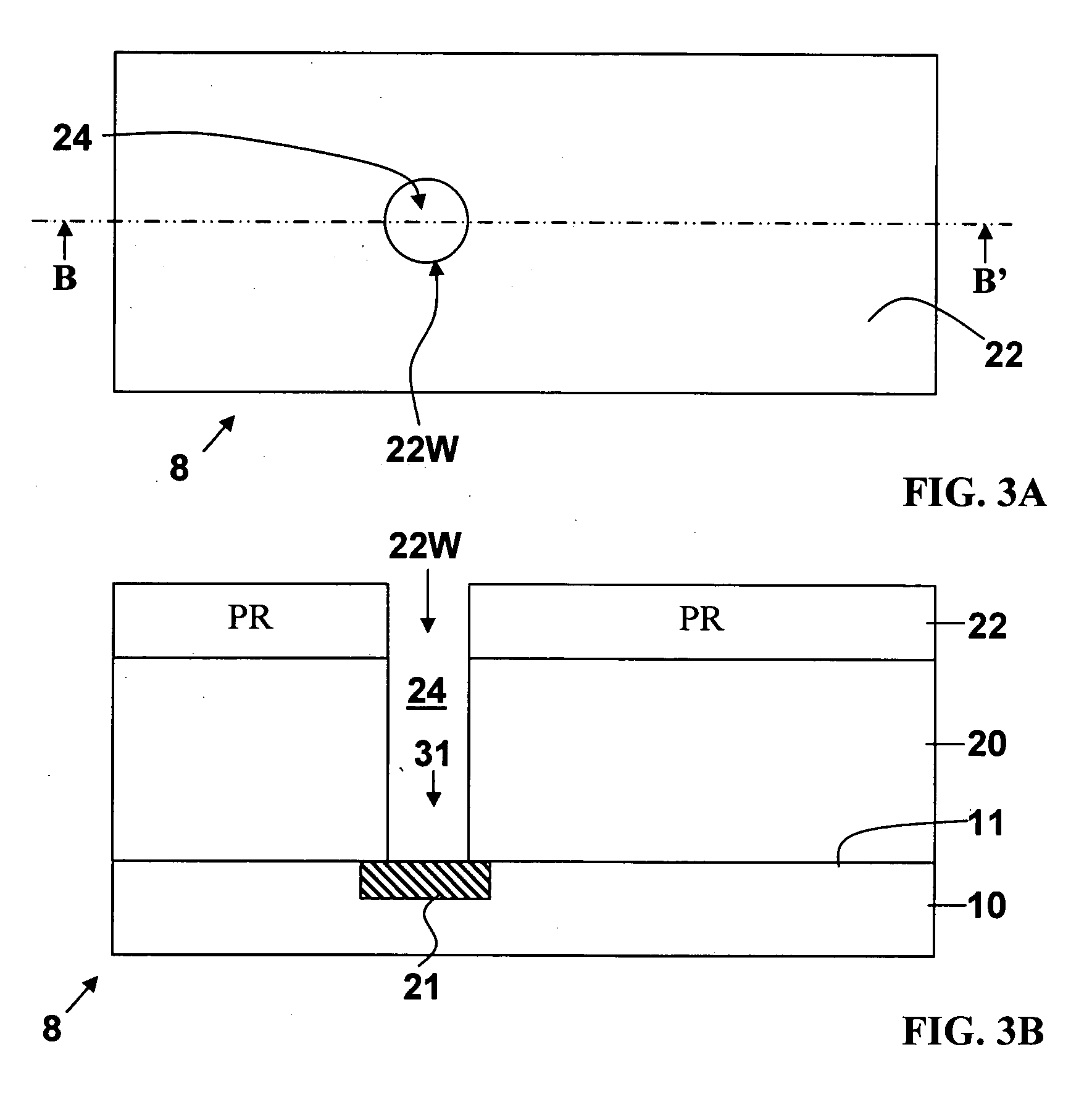
[0042] The present invention provides an improved Phase Change Memory (PCM) cell structure. By reducing the contact area between the phase change material of the PCM cell and one of the electrodes connected thereto, the resulting high current density can induce the necessary heating and phase changes within the PCM effectively with relatively low current (and, thus, low operating power).

[0043] Prior art structures often attempt to realize this method of operating power reduction, but are hampered by complex integration schemes and designs that can result in poor uniformity across arrays of the memory elements. Uniformity is necessary to ensure each element can be switched with the same characteristic current pulse, and, although less difficult with PCM, to ensure that each element's readout resistance is in a desired range for a “high” state and a “low” state—without the two states overlapping. Complex integration schemes are undesirable because they are expensive, and offer greate...


PUM


Abstract

A PCM cell structure comprises a first electrode, a phase change element, and a second electrode, wherein the phase change element is inserted in between the first electrode and the second electrode and only the peripheral edge of one of the first and second electrodes contacts the phase change element thereby reducing the contact area between the phase change element and one of the electrodes thereby increasing the current density through the phase change element and effectively inducing the phase change at a first programming power.

Description

FIELD OF THE INVENTION [0001] The present invention relates to memory devices, and more particularly a Phase Change Memory (PCM) cell structure and methods of making and using the same. BACKGROUND [0002] Recently nonvolatile chalcogenide Random Access Memory (RAM) devices, made of the germanium-antimony-tellurium (Ge2Sb2Te5) chalcogenide material, have been regarded as the most promising next-generation memory devices. The term “chalcogen” refers to the Group VI elements of the periodic table; and the term “chalcogenide” refers to alloys containing at least one of these elements, e.g. the alloy of germanium, antimony, and tellurium, etc. Chalcogenide materials have been used in PCM devices, especially in both rewritable Compact Disk (CD) and Digital Video Disk or Digital Versatile Disc (DVD) devices. This kind of memory when introduced into semiconductor chips has many advantages over others in areas, e.g. scalability, high sensing margin, low energy consumption, and cycling enduran...

Claims


Application Information

Patent Timeline
IPC IPC(8): H01L29/02
CPCH01L45/06H01L45/122H01L45/1675H01L45/126H01L45/144H01L45/1233H10N70/231H10N70/821H10N70/826H10N70/8413H10N70/8828H10N70/063
Inventor ARNOLD, JOHNCLEVENGER, LAWRENCEDALTON, TIMOTHYGAIDIS, MICHAELHSU, LOUISRADENS, CARLWONG, KEITHYANG, CHIH-CHAO
Owner IBM CORP
Why Eureka
Try Eureka