CMOS structures and methods for improving yield

a technology of cmos and structures, applied in the field of cmos structures and methods for improving yield, can solve the problems of becoming even more difficult to etch contact holes, and difficult to deal with dsl boundaries, so as to improve the yield of cmos devices, improve the yield of chips, and improve the effect of efficiency and economics

Inactive Publication Date: 2007-11-01
ELPIS TECH INC
View PDF102 Cites 47 Cited by
  • Summary
  • Abstract
  • Description
  • Claims
  • Application Information

AI Technical Summary

Benefits of technology

[0011]The present invention provides a simple, effective and economical method to improve the yield of CMOS devices using contact etch stopper liner, including neutral stressed liner, single stressed liner and DSL, technology. In order to improve the chip yield, the present invention provides a method in which a sputter etching process is employed to smooth/flatten (i.e., thin) the top surface of the stressed (neutral, single and dual) liner(s). When DSL techn

Problems solved by technology

However, with aggressive scaling of contacted gate pitch, it becomes more difficult to deal with DSL boundaries, especially for etching contact-to-active-area (CA) holes.
In addition to the above, current technology provides a large aspect ratio between the height of the gate liner top and the pitch of t

Method used


Image

  • CMOS structures and methods for improving yield
  • CMOS structures and methods for improving yield
  • CMOS structures and methods for improving yield

Examples


first embodiment

[0049]Reference is first made to FIGS. 1-4B which are pictorial representations through various cross sectional views illustrating basic processing steps of the present invention.

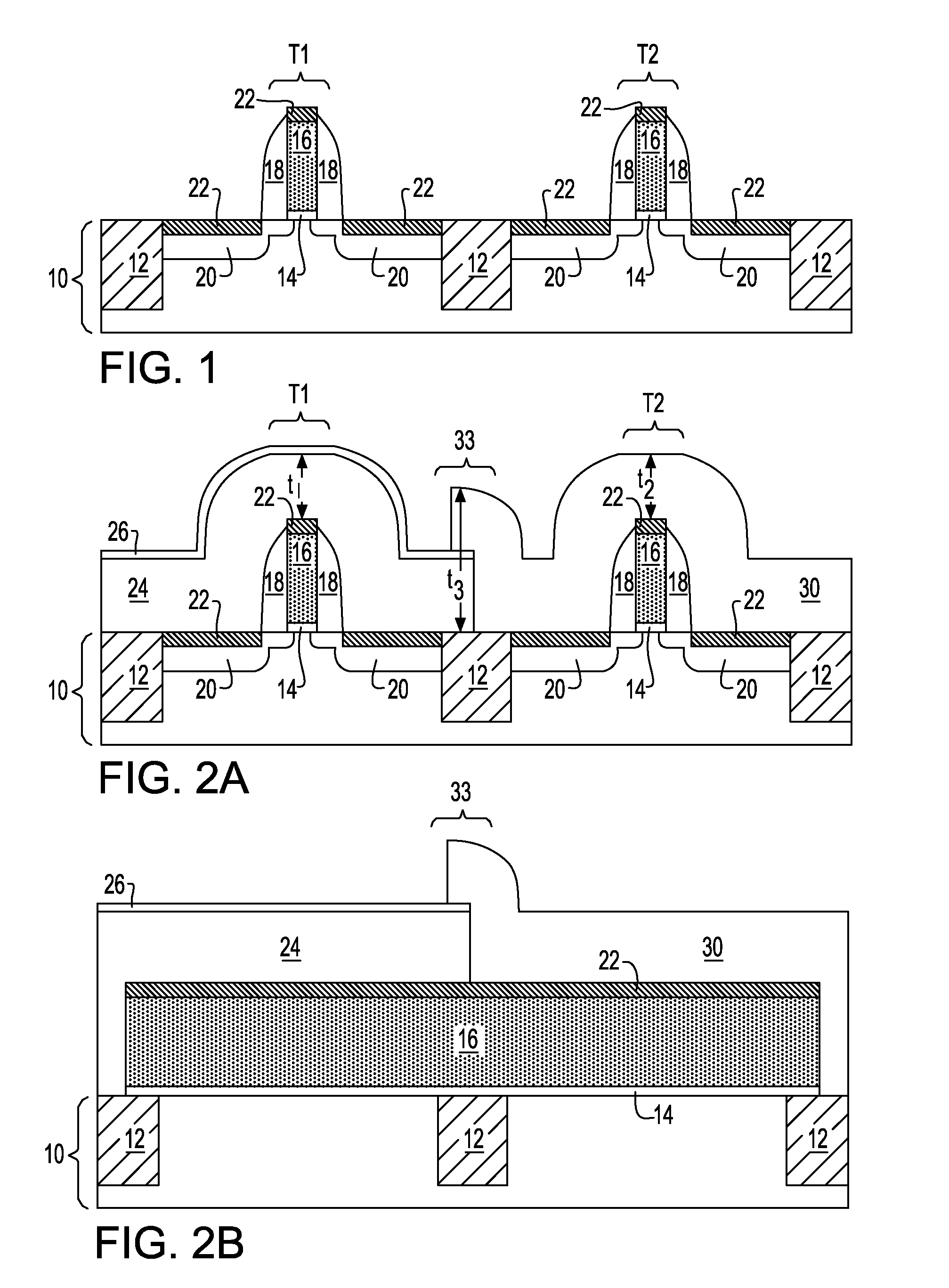
[0050]Specifically, FIG. 1 shows a semiconductor substrate 10 that comprises active regions separated by an isolation region 12. A first transistor T1 is located upon one active region and a second transistor T2 is located upon an adjacent active region. Transistors T1 and T2 are of different polarity (i.e., conductivity type) and thus the doping type in each of active regions is different. The transistors T1 and T2 comprise gate dielectrics 14 located upon the active regions of the semiconductor substrate 10. Gate electrodes 16 are aligned upon gate dielectrics 14, although such alignment is not a requirement of the invention. At least one spacer 18 adjoins each of the gate electrodes 16. Source / drain regions 20 are located within the active regions of the semiconductor substrate and separated by channel r...

second embodiment

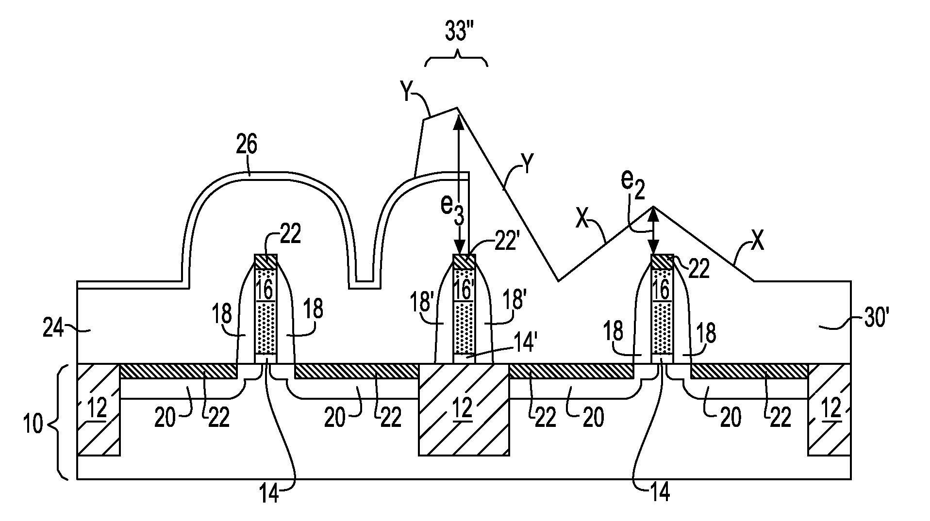
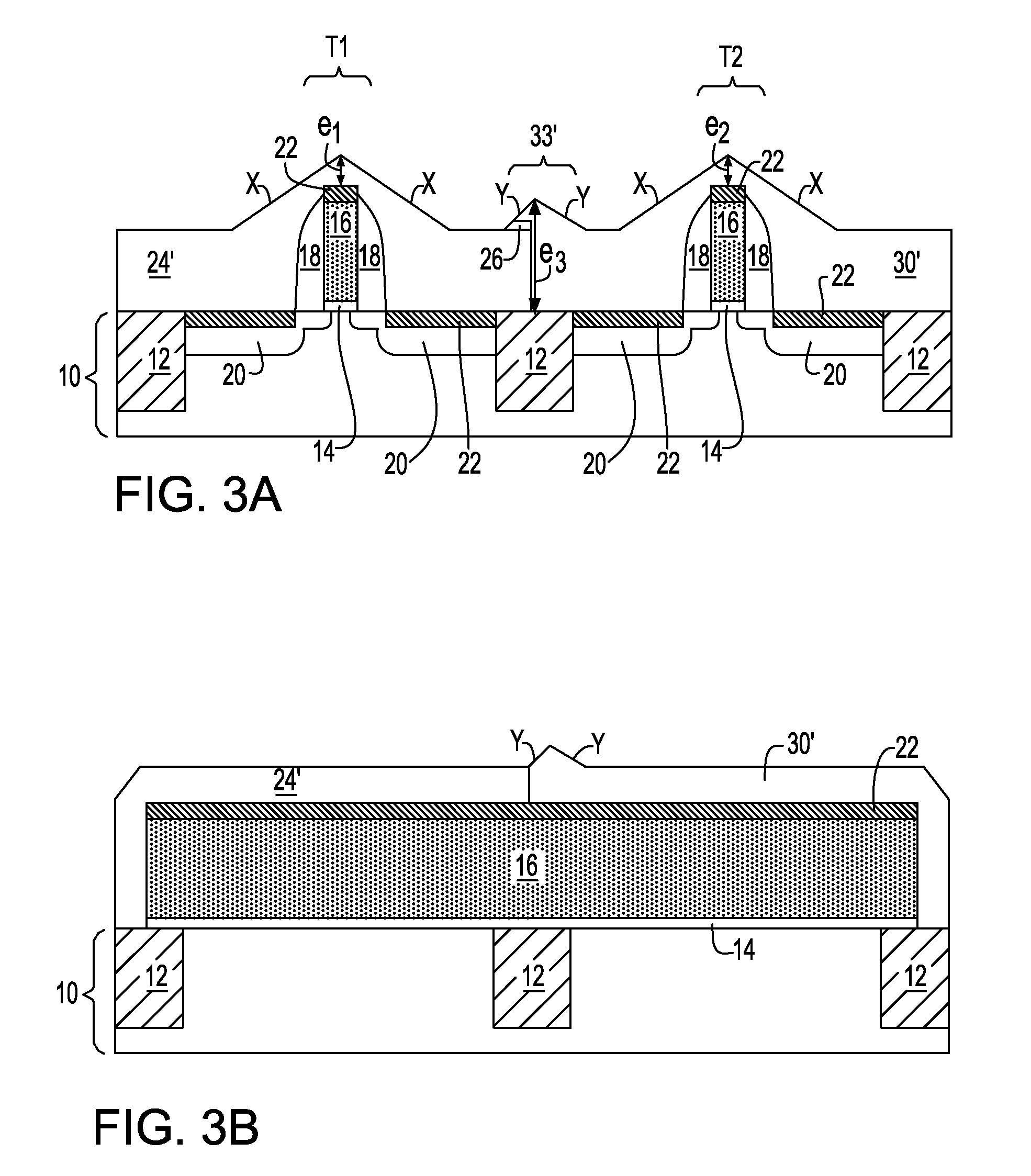
[0090]FIGS. 6A-6B shows a CMOS structure in accordance with the invention. The CMOS structure comprises complementary first etched stressed layer 24′ located upon first transistor T1 and second etched stressed layer 30′ located upon second transistor T2. The complementary first etched stressed layer 24′ and second etched stressed layer 30′ overlap at a location interposed between the first transistor T1 and the second transistor T2. The size of the etched overlap region 33′ is smaller than that for a structure prepared utilizing a conventional DSL process. Additionally, the first etched stressed layer 24′ and the second etched stressed layer 30′ are smoother and thinner as compared to that of a conventional DSL-containing CMOS structure. That is, the first and second etched stressed layers (24′ and 30′, respectively) have an etched thickness over their corresponding transistor that is less than the thickness of the deposited and non-etched stressed layers. Also, each of the etched s...

third embodiment

[0095]FIGS. 9A-9B illustrate the structure in accordance with the present invention. Specifically, the structure includes a single etched stressed layer 50′ located upon the first transistor T1 and the second transistor T2. The single etched stressed layer 50′ is smoother and thinner as compared to that of a conventional single stress liner-containing CMOS structure. That is, the etched stressed layer 50′ has an etched thickness over the transistors that is less than the thickness of the deposited and non-etched stressed layers. Also, the etched stressed layer 50′ over each of the transistors has tapered surface sidewalls X that meet each other typically forming an inverted V-shape.

[0096]FIGS. 10A-11B are pictorial representations through various cross sections illustrating the basic processing steps in accordance with a fourth embodiment of the invention. The fourth embodiment of the present invention begins by first providing the structure which is shown in FIGS. 8A-8B of the thir...


PUM


Abstract

A simple, effective and economical method to improved the yield of CMOS devices using contact etching stopper liner, including, single neutral stressed liner, single stressed liner and dual stress liner (DSL), technology is provided. In order to improve the chip yield, the present invention provides a method in which a sputter etching process is employed to smooth/flatten (i.e., thin) the top surface of the contact etch stopper liners. When DSL technology is used, the inventive sputter etching process is used to reduce the complexity caused by DSL boundaries to smooth/flatten top surface of the DSL, which results in significant yield increase. The present invention also provides a semiconductor structure including at least one etched liner.

Description

RELATED APPLICATIONS[0001]This application is a continuation-in-part (CIP) application of co-pending and co-assigned U.S. application Ser. No. 11 / 380,695, filed Apr. 28, 2006, the entire contents of which are incorporated herein by reference.FIELD OF THE INVENTION[0002]The present invention relates to semiconductor structures and methods of fabricating the same. More particularly, the invention relates to semiconductor structures and methods that provide mechanical stress within complementary metal oxide semiconductor (CMOS) structures to enhance device performance and improve chip yield.BACKGROUND OF THE INVENTION[0003]CMOS structures comprise complementary mated pairs of field effect transistors of differing conductivity type. Due to the use of complementary mated pairs of differing conductivity type, CMOS structures also provide for reduced energy or power consumption.[0004]A trend within CMOS fabrication is the use of stressed layers as a means to produce a mechanical stress or ...

Claims


Application Information

Patent Timeline
IPC IPC(8): H01L21/76H01L27/12
CPCH01L21/823807H01L29/7843H01L21/823871H01L21/823864H01L21/31116
Inventor ZHU, HUILONGYANG, DAEWON
Owner ELPIS TECH INC
Why Eureka
Try Eureka