Adaptive Bias Current Circuit and Method for Amplifiers

a bias current and amplifier technology, applied in the field of amplifiers, can solve the problems of stringent and challenging linearity requirements of radio frequency, amplifiers in rf circuits that consume considerable power, and achieve the effect of substantial current boos

Active Publication Date: 2007-11-01
RGT UNIV OF CALIFORNIA
View PDF4 Cites 27 Cited by
  • Summary
  • Abstract
  • Description
  • Claims
  • Application Information

AI Technical Summary

Benefits of technology

[0010] The invention provides an adaptive bias method and circuits for amplifiers that provide a substantial current boost at least partly based upon a sensed input power of an amplifier circuit. Methods and circuits of the invention provide an additional bias current based upon the sensed input power. Circuits of the invention may be simple, area-efficient, low-power, stable and digitally-programmable. In addition, methods and circuits of the invention may be used with a number of amplifier circuit configurations, including amplifiers having either inductor and / or resistive degeneration.

Problems solved by technology

The RF circuits of a portable device, however, present one of biggest demands on the power source of a portable device.
In particular, the amplifiers in RF circuits consume considerable power.
This often translates to stringent and challenging linearity requirements for the radio frequency (RF) amplifiers, which constitute the end of the transmitter chain and are tasked to handle the highest signal levels.
Another important, although conflicting, design criteria is the amplifier power consumption.
Achieving efficiency during both conditions has proved difficult in practice.
Recognized problems with these and other amplifier circuits using inductors include the amount of real estate occupied by the inductors.
Any increase in the base current of the common-emitter amplifier thus causes a voltage drop at the base.
The subsequent base-emitter voltage (Vbe) reduction at large signal conditions greatly limits the current boost.
Inductor degeneration avoids raising the emitter voltage, but, as mentioned above, inductors present fabrication problems due to the amount of real estate required to accommodate inductors.

Method used


Image

  • Adaptive Bias Current Circuit and Method for Amplifiers
  • Adaptive Bias Current Circuit and Method for Amplifiers
  • Adaptive Bias Current Circuit and Method for Amplifiers

Examples


Embodiment Construction

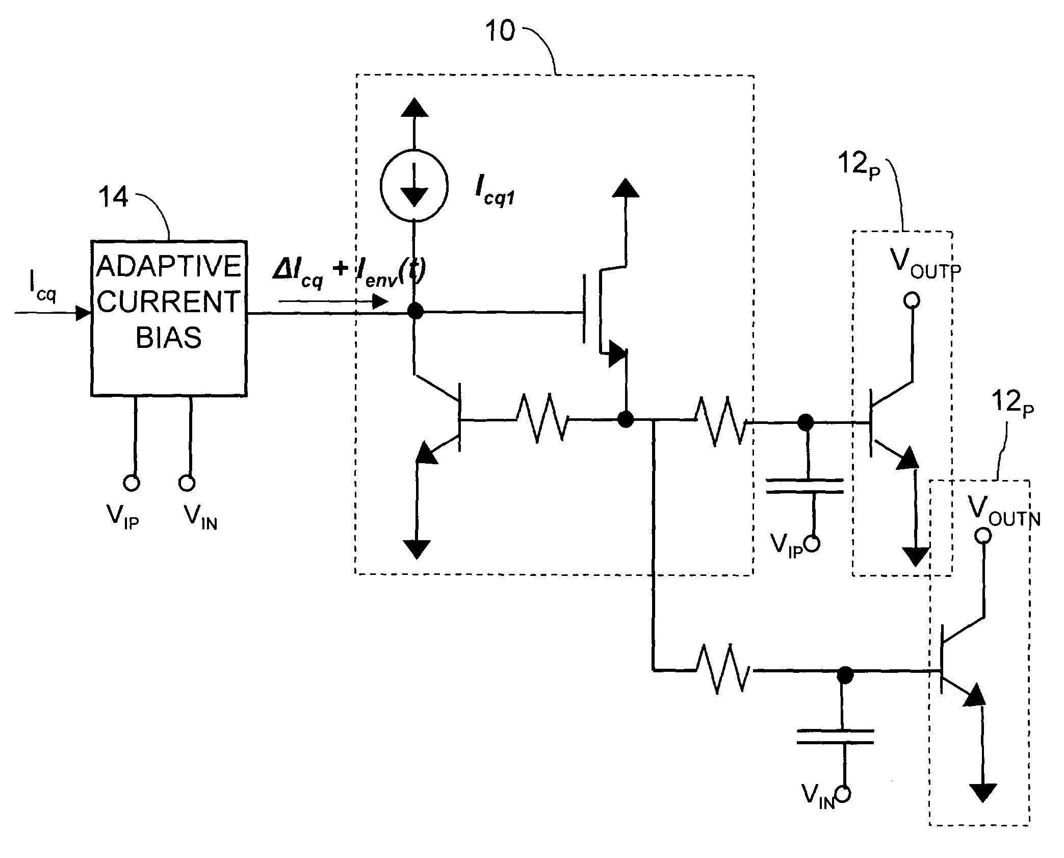
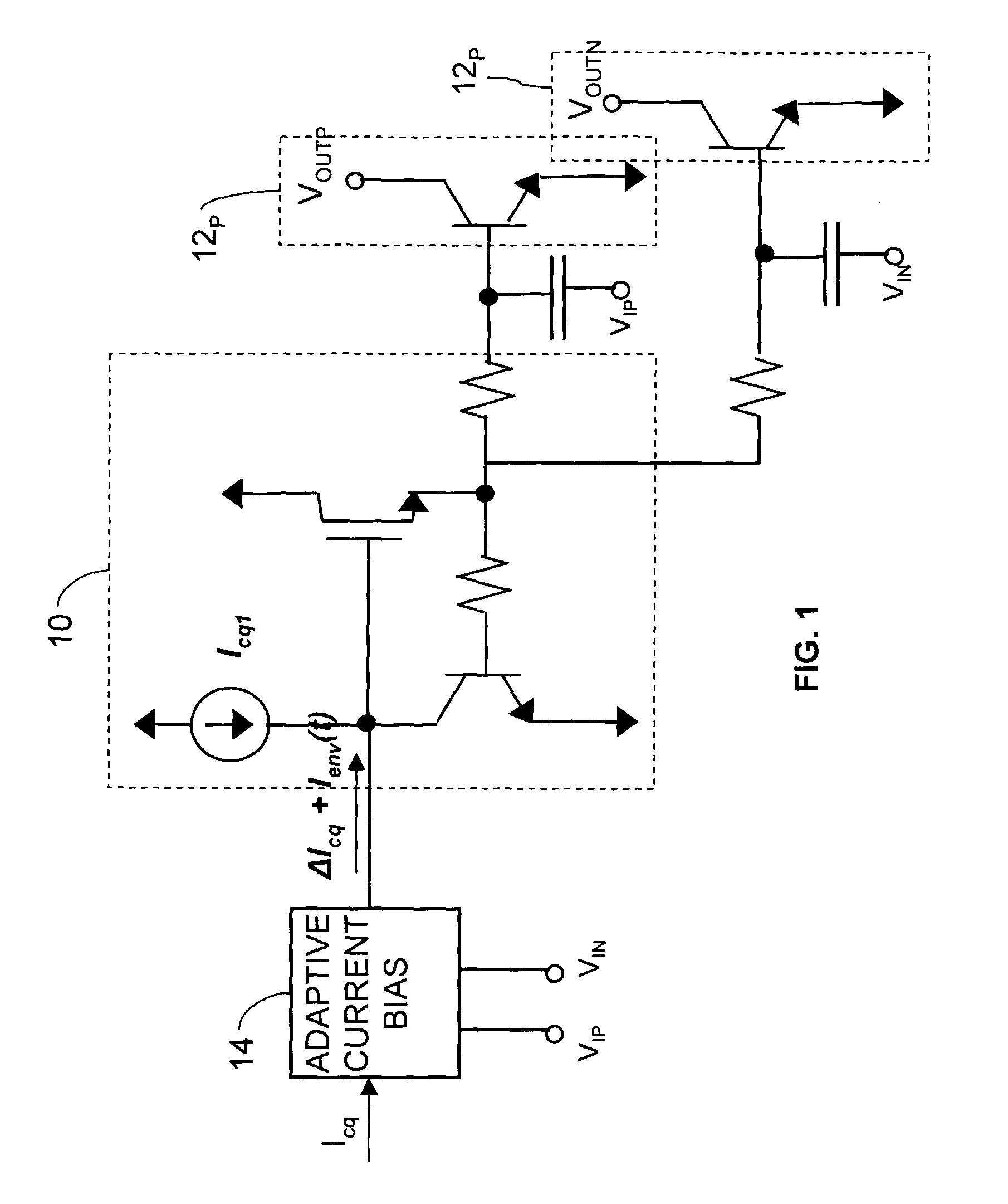
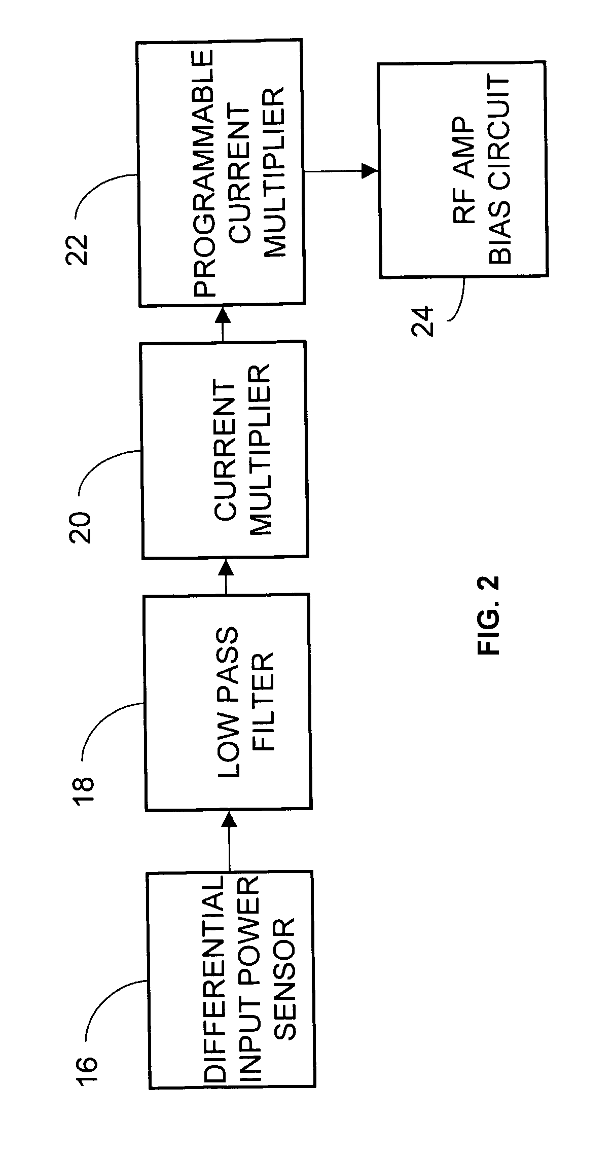
[0015] Embodiments of the invention provide an input power based current boost to the bias circuit of an RF amplifier. In preferred embodiments of the invention, a differential transistor pair senses the input power difference of the positive and negative input voltages of an RF amplifier. As input power to the differential RF amplifier increases, the output current of the differential transistor pair clips, providing for high average current responsive to the level of input power. The differential transistors are biased with low quiescent current, so that their collector currents will be clipped during large-signal conditions, thus raising their average (dc) collector currents above the quiescent level. A low pass filter removes harmonics, and a current boost ΔI that is proportional to the input power is produced. This current boost is provided to the bias circuit of the RF amplifier. Preferably, one or more current mirrors, including a digitally programmable current mirror are pro...


PUM


Abstract

An adaptive bias method and circuits for amplifiers that provide a substantial current boost based at least partly upon a sensed input power of an amplifier circuit. Methods and circuits of the invention provide an additional bias current based upon the sensed input power. Circuits of the invention may be simple, area-efficient, low-power, stable and digitally-programmable. In addition, methods and circuits of the invention may be used with a number of amplifier circuit configurations, including amplifiers having either inductor and / or resistive degeneration.

Description

TECHNICAL FIELD [0001] A general field of the invention is amplifiers. A particular field of the invention is radio frequency (RF) amplifiers, e.g., amplifiers utilized in handsets and other devices that receive and transmit RF signals and typically use portable power supplies. BACKGROUND ART [0002] Efficient amplifiers are important for RF applications. A typical RF device uses a portable power source, e.g., a battery. The operation of the RF device is enhanced when the demand on the battery is reduced. The RF circuits of a portable device, however, present one of biggest demands on the power source of a portable device. In particular, the amplifiers in RF circuits consume considerable power. [0003] There are different methods of RF signal transmission. In some methods, the information to be transmitted is completely coded in the phase of the RF signals that are transmitted. GSM is an exemplary standard in which the information to be transmitted is completely coded in the phase of ...

Claims


Application Information

Patent Timeline
Patent Type & Authority Applications(United States)
IPC IPC(8): H03F3/189H03G3/20
CPCH03F1/0266H03F1/22H03F3/19H03F3/4508H03F2200/18H03F2203/45481H03F2200/465H03F2203/45112H03F2203/45154H03F2203/45394H03F2200/451H03F3/04
Inventor LEUNG, VINCENTGUDEM, PRASAD S.LARSEN, LAWRENCE E.
Owner RGT UNIV OF CALIFORNIA
Why Eureka
Try Eureka