

Polishing Apparatus and Polishing Method
a technology of polishing apparatus and polishing rate, which is applied in the direction of grinding machine components, manufacturing tools, lapping machines, etc., can solve the problems of affecting the uniformity of the polishing rate, the difficulty of uniform supply of a chemical liquid (slurry) to an entire surface of the wafer, and the problem of increasing the electric capacity between adjacent interconnections, so as to achieve uniform supply of chemical liquid and uniform polishing rate.
- Summary
- Abstract
- Description
- Claims
- Application Information
AI Technical Summary
Benefits of technology
Problems solved by technology
Method used
Image

Examples
first embodiment
[0142]FIG. 10 is a schematic view showing a polishing apparatus 30 according to the present invention. As shown in FIG. 10, the polishing apparatus 30 includes a polishing table 34 having a polishing surface 32 attached on an upper surface thereof, a top ring 36 for holding a workpiece such as a semiconductor wafer W on a lower surface thereof, a top ring head 40 pivotable about a pivot shaft 38, a chemical liquid supply nozzle 42 which serves as a chemical liquid supply mechanism for supplying a chemical liquid (polishing liquid) onto the polishing surface 32, and a controller 44 for controlling operation of the polishing apparatus 30. The polishing surface 32 on the polishing table 34 is formed by polyurethane foam, a fixed abrasive, or an impregnated abrasive.
[0143] The polishing table 34 is coupled to a motor 46 located below the polishing table 34 and rotated by the motor 46. Thus, the motor 46 serves as a rotation mechanism to rotate the polishing table 34 and the polishing su...
second embodiment
[0203]FIG. 18 is a schematic view showing a polishing apparatus 300 according to the present invention. The polishing apparatus 300 perform a composite electrolytic polishing process. The polishing apparatus 300 has a cylindrical electrolytic cell 302 having a bottom and a top ring 304 disposed above the electrolytic cell 302. The electrolytic cell 302 has an opening at an upper portion thereof and holds an electrolytic solution 301 therein. The top ring 304 detachably holds a semiconductor wafer W in a state such that the semiconductor wafer W faces downward. The electrolytic solution 301 may comprise a chemical liquid including an oxidizer, a chelating agent, and abrasive particles.
[0204] The electrolytic cell 302 is coupled directly to the main shaft 306, which is rotated by a rotation mechanism such as a motor. A cathode plate (electrode) 308 is disposed horizontally at a lower portion of the electrolytic cell 302 and immersed in the electrolytic solution 301. The cathode plate ...
third embodiment
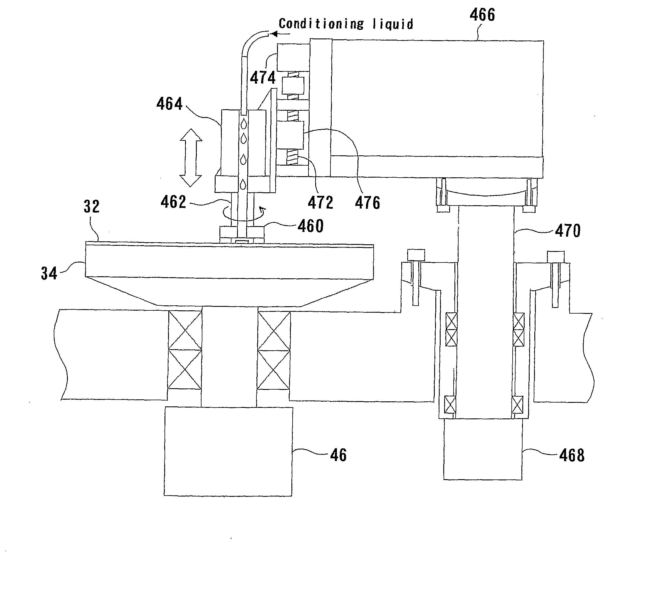
[0218]FIG. 19 is a schematic view showing a polishing apparatus 430 according to the present invention. As shown in FIG. 19, the polishing apparatus 430 includes a polishing table 34 having a polishing surface 32 attached on an upper surface thereof, a top ring 36 for holding a workpiece such as a semiconductor wafer W on a lower surface thereof, a top ring head 40 pivotable about a pivot shaft 38, a chemical liquid supply nozzle 42 which serves as a chemical liquid supply mechanism for supplying a chemical liquid (polishing liquid) onto the polishing surface 32, and a controller 44 for controlling operation of the polishing apparatus 30. The polishing surface 32 on the polishing table 34 is generally formed by resin of polyurethane foam, a fixed abrasive, or an impregnated abrasive.
[0219] The polishing table 34 is coupled to a motor 46 located below the polishing table 34 and rotated by the motor 46. Thus, the motor 46 serves as a rotation mechanism to rotate the polishing table 34...
PUM
| Property | Measurement | Unit |
|---|---|---|
| relative speed | aaaaa | aaaaa |
| pressure | aaaaa | aaaaa |
| relative permittivity | aaaaa | aaaaa |
Abstract
Description
Claims
Application Information