
Method for Forming Ti Film and Tin Film, Contact Structure, Computer Readable Storing Medium and Computer Program

Inactive Publication Date: 2007-11-08
TOKYO ELECTRON LTD
View PDF5 Cites 30 Cited by
  • Summary
  • Abstract
  • Description
  • Claims
  • Application Information

AI Technical Summary

Benefits of technology

[0010] An object of the present invention is to provide a film formation method for forming a Ti film and a TiN film, which can decrease the contact resistance and can suppress the film peeling, even where the film formation is performed at a low temperature in forming the Ti film and TiN film on an underlayer, such as an Si substrate or a metal silicide film disposed on a substrate. This object of the present invention is further conceived to provide a contact structure formed by such a film formation method, and a computer readable storage medium and a computer program for performing control to execute such a film formation method.
[0023] According to the present invention, a Ti film and a TiN film are formed on an underlayer comprising an Si substrate or a metal silicide film, such as a nickel silicide (NiSi), disposed on a substrate. Before the Ti film is formed, the surface of the underlayer is cleaned by a suitable method. Then, the Ti film is formed to have a film thickness of not less than 2 nm but less than 10 nm on the underlayer by CVD using a Ti compound gas. In this case, a reaction layer of Ti with the underlayer is preferably formed to decrease the contact resistance. Further, the Ti film is prepared to be sufficiently nitrided. Consequently, even where the film formation is performed at a low temperature, it is possible to decrease the contact resistance and to effectively prevent the film peeling on the Ti film.
[0024] When the TiN film is formed, a first step and a second step may be alternately repeated a plurality of times. The first step is arranged to supply a Ti compound gas and a gas containing N and H. The second step is arranged to stop the Ti compound gas and supply the gas containing N and H. Accordingly, a TiN film formed in the first step is efficiently subjected to dechlorination by annealing in the second step. In this case, even where the film formation is performed at a low temperature, the TiN film is formed to have good film quality with little residual chlorine and a low resistivity. Consequently, it is possible to more effectively suppress occurrence of cracks in the TiN film, and to reliably prevent film peeling of the TiN film.
[0025] The cleaning process for the surface of the underlayer may be performed by sputter etching by use of plasma before the Ti film is formed. In this case, natural oxide films on the surface of the underlayer are efficiently removed to improve the reactivity between the surface of the underlayer and Ti.
[0026] The cleaning process for the surface of the underlayer may be performed by use of a gas excited by, e.g., remote plasma. In this case, the cleaning process is performed mainly by a chemical action, and the underlayer is less damaged during the cleaning process. Reaction products formed due to the chemical action are then thermally decomposed and sublimated by, e.g., a heat process. Consequently, the natural oxide films on the surface of the underlayer can be completely removed.

Problems solved by technology

This etching action brings about a problem such that the TiN film peels off the Ti film due to an insufficient adhesion degree between the Ti film and the upper layer or TiN film, and a thermal stress or the like applied when a filler metal film is formed.
Further, in recent years, due to miniaturization of devices, impurity diffusion layers formed in Si substrates have become thinner.
However, Patent Document 1 described above pays no attention to such low temperature film formation.
Specifically, when the nitriding process is performed after the Ti film formation, the Ti film is not sufficiently nitrided.
Consequently, the TiN film may peel off the Ti film due to an insufficient adhesion degree between the Ti film and the upper layer or TiN film, and a thermal stress or the like applied when a filler metal film is formed.

Method used


Image

  • Method for Forming Ti Film and Tin Film, Contact Structure, Computer Readable Storing Medium and Computer Program
  • Method for Forming Ti Film and Tin Film, Contact Structure, Computer Readable Storing Medium and Computer Program
  • Method for Forming Ti Film and Tin Film, Contact Structure, Computer Readable Storing Medium and Computer Program

Examples


Embodiment Construction

[0046] Embodiments of the present invention will now be described with reference to the accompanying drawings.

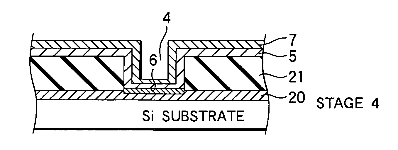
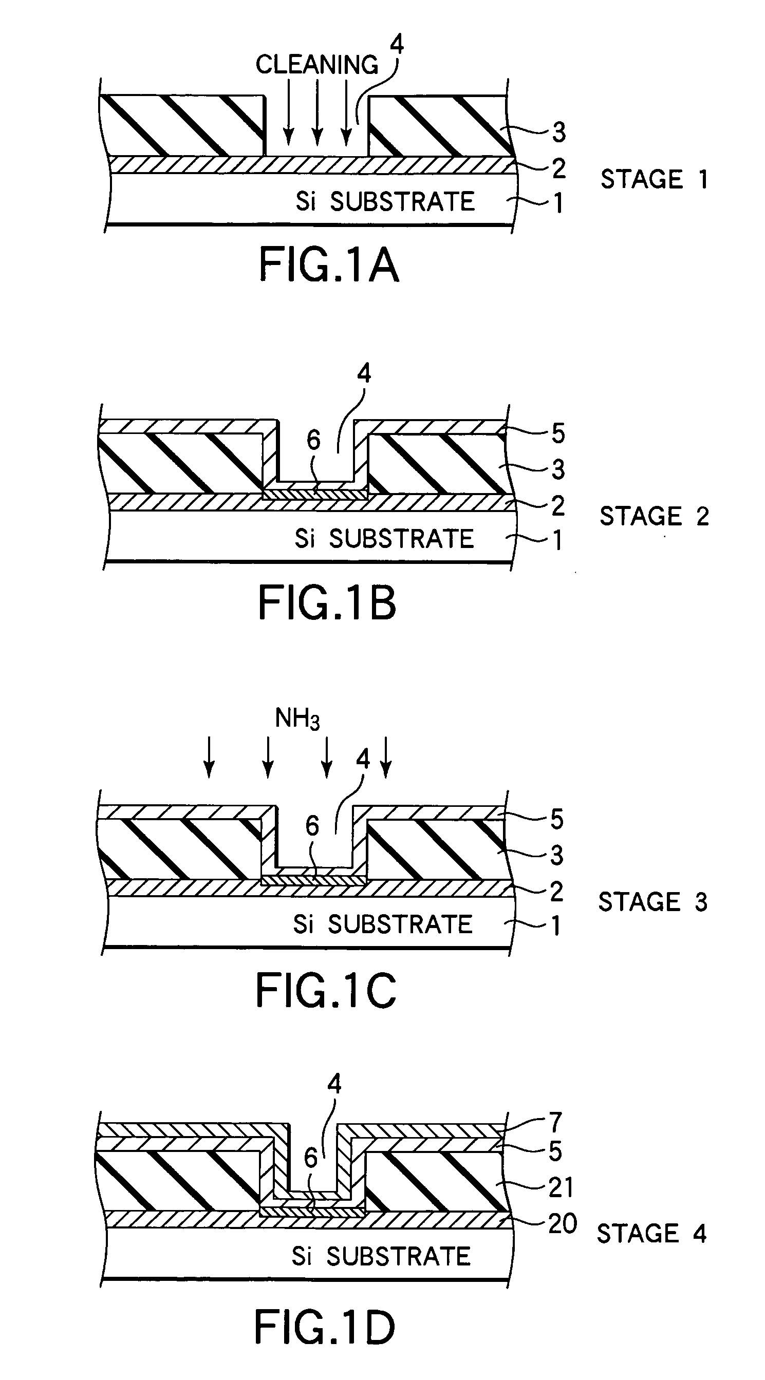
[0047]FIGS. 1A to 1D are process views for explaining a method for forming a Ti film and a TiN film according to an embodiment of the present invention.

[0048] As shown in FIG. 1A, a metal silicide film, such as a nickel silicide (NiSi) film 2, is disposed on a semiconductor substrate, such as an Si substrate 1. An inter-level insulating film 3 is disposed on the nickel silicide film 2, and is provided with a contact hole 4 formed therein and reaching the nickel silicide film 2. In this state, at first, the surface of the nickel silicide film 2 is cleaned by removing natural oxide films, which are very thin, and so forth present thereon to obtain an active and clean surface (stage 1). This operation improves the reactivity between the nickel silicide and Ti.

[0049] The cleaning process used at this time can be selected from various methods, such as (1) sputter etching by us...


PUM

PropertyMeasurementUnit
Temperatureaaaaaaaaaa
Thicknessaaaaaaaaaa
Thicknessaaaaaaaaaa

Abstract

A cleaning process is performed on the surface of a nickel silicide film serving as an underlayer. Then, a Ti film is formed to have a film thickness of not less than 2 nm but less than 10 nm by CVD using a Ti compound gas. Then, the Ti film is nitrided. Then, a TiN film is formed on the Ti film thus nitrided, by CVD using a Ti compound gas and a gas containing N and H.

Description

TECHNICAL FIELD [0001] The present invention relates to a film formation method for forming a Ti film and a TiN film, and a contact structure, which are used in contact holes and via-holes of semiconductor devices. The present invention further relates to a computer readable storage medium and a computer program. BACKGROUND ART [0002] In manufacturing semiconductor devices, as higher density and higher integration degree are required to the devices, multi-layered wiring structures are being increasingly used for circuitry. Under the circumstances, embedding techniques for electrical connection between layers have become important, for example, at contact holes used as connection portions between an Si substrate or poly-crystalline silicon layer on the lower side and wiring layers on the upper side, and at via-holes used as connection portions between upper and lower wiring layers. [0003] In general, a metal, such as Al or W, or an alloy made mainly of these materials is used as a ma...

Claims


Application Information

Patent Timeline
IPC IPC(8): H01L23/48H01L21/44C23C16/02C23C16/14C23C16/34H01L21/02H01L21/28H01L21/285H01L21/3205H01L21/768
CPCC23C16/0281C23C16/34H01J37/321H01L21/02063H01L21/76856H01L21/32051H01L21/76814H01L21/76846H01L21/28556Y10S438/905Y10S438/906Y10S438/974H01L21/20H01L21/28
Inventor TADA, KUNIHIRONARUSHIMA, KENSAKUWAKABAYASHI, SATOSHI
Owner TOKYO ELECTRON LTD
Learn More