In-situ formation of oxidized aluminum nitride films

a technology film, which is applied in the field of in-situ formation of oxidized aluminum nitride (aln) films, can solve the problems of no longer practicable siosub>2 /sub>scaling, and achieve the effect of increasing the dielectric constant of aluminum nitride films and no increase in aluminum nitride film thickness

Active Publication Date: 2007-11-08
TOKYO ELECTRON LTD
View PDF2 Cites 15 Cited by
  • Summary
  • Abstract
  • Description
  • Claims
  • Application Information

AI Technical Summary

Benefits of technology

[0009]According to one embodiment of the invention, the method includes providing the substrate in a process chamber, depositing an AlN film on the substrate, and post-treating the AlN film with exposure to a nitrogen and oxygen-containing gas. The post-treating increases the dielectric constant of the aluminum nitride film with substantially no increase in the aluminum nitride film thickness. The method can also include pre-treating the substrate prior to AlN deposition, annealing the AlN film before or after post-treating, or both.

Problems solved by technology

These exemplary high-k materials, and nanolaminates thereof, can be used in many logic and memory devices where the scaling of SiO2 is no longer practical.

Method used


Image

  • In-situ formation of oxidized aluminum nitride films
  • In-situ formation of oxidized aluminum nitride films
  • In-situ formation of oxidized aluminum nitride films

Examples


Embodiment Construction

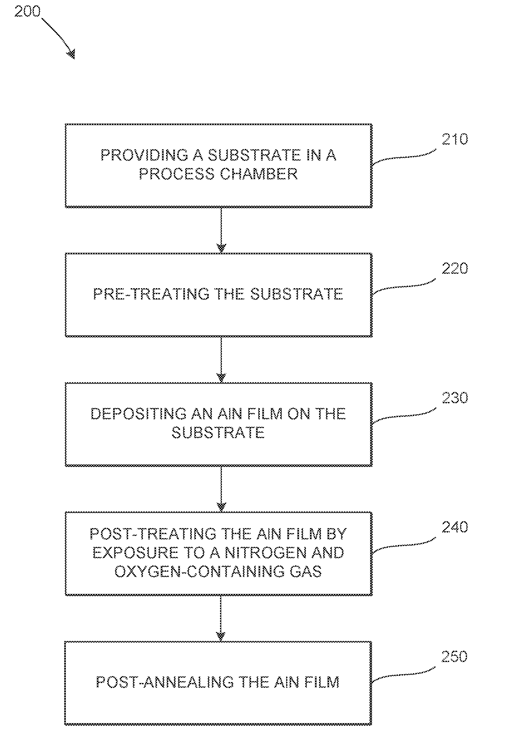
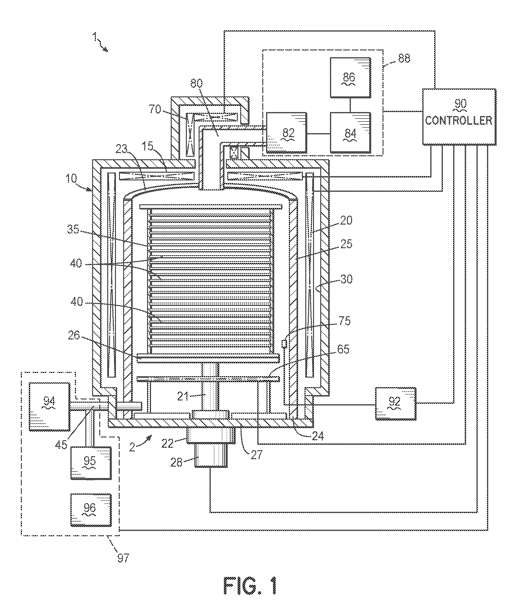
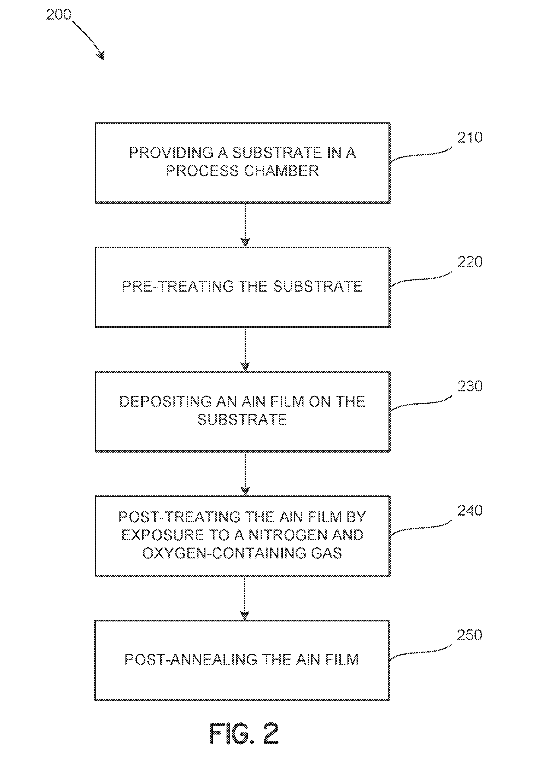
[0017]Embodiments of the invention provide a method for forming high dielectric constant oxidized AlN films with good physical and electrical properties. AlN is a high-k dielectric material with a wide band gap. AlN has good thermal and chemical stability and may be utilized as a gate dielectric and / or a diffusion barrier in a gate electrode structure. AlN has a relatively high dielectric constant with reported values between 6 and 18.

[0018]According to one embodiment of the invention, a method is provided for processing a substrate by providing the substrate in a process chamber, depositing an AlN film on the substrate, and post-treating the AlN film with exposure to a nitrogen and oxygen-containing gas, where the post-treating increases the dielectric constant of the AlN film without substantially increasing the thickness of the AlN film. The post-treated AlN has smooth film interfaces, good film uniformity across a wafer, low film interface trap densities, high dielectric constan...


PUM

PropertyMeasurementUnit
temperatureaaaaaaaaaa

Abstract

A method is provided for in-situ formation of a thin oxidized AlN film on a substrate. The method includes providing the substrate in a process chamber, depositing an AlN film on the substrate, and post-treating the AlN film with exposure to a nitrogen and oxygen-containing gas. The post-treating increases the dielectric constant of the AlN film with substantially no increase in the AlN film thickness. The method can also include pre-treating the substrate prior to AlN deposition, post-annealing the AlN film before or after the post-treatment, or both.

Description

CROSS-REFERENCE TO RELATED APPLICATION[0001]The present invention claims benefit of and priority to U.S. Provisional Application No. 60 / 746,750, filed May 8, 2006, which is incorporated by reference herein in its entirety.FIELD OF THE INVENTION[0002]The present invention relates to formation of high dielectric constant films, and more particularly, to in-situ formation of oxidized aluminum nitride (AlN) films.BACKGROUND OF THE INVENTION[0003]Several methods have been developed for creating thin films on substrates used in manufacturing semiconductor devices. Among the more established techniques is Chemical Vapor Deposition (CVD). Atomic Layer Deposition (ALD), also referred to Molecular Layer Deposition (MLD), a variant of CVD, is a relatively newer technology now emerging as a potentially superior method of achieving uniform, conformal film deposition. ALD has demonstrated an outstanding ability to maintain ultra-uniform thin deposition layers over complex topology. This is at lea...

Claims


Application Information

Patent Timeline
Patent Type & Authority Applications(United States)
IPC IPC(8): H01L21/31H01L21/469
CPCC23C16/56C23C16/303
Inventor REID, KIMBERLY G.DIP, ANTHONY
Owner TOKYO ELECTRON LTD
Why Eureka
Try Eureka