
Measuring layer thickness or composition changes

a technology of composition change and layer thickness, applied in the direction of mechanical measuring arrangement, semiconductor/solid-state device testing/measurement, instruments, etc., can solve the problems of inability to work with in situ measurement, and inability to achieve in situ measuremen

Active Publication Date: 2007-11-08
GLOBAL OLED TECH
View PDF10 Cites 28 Cited by
  • Summary
  • Abstract
  • Description
  • Claims
  • Application Information

AI Technical Summary

Benefits of technology

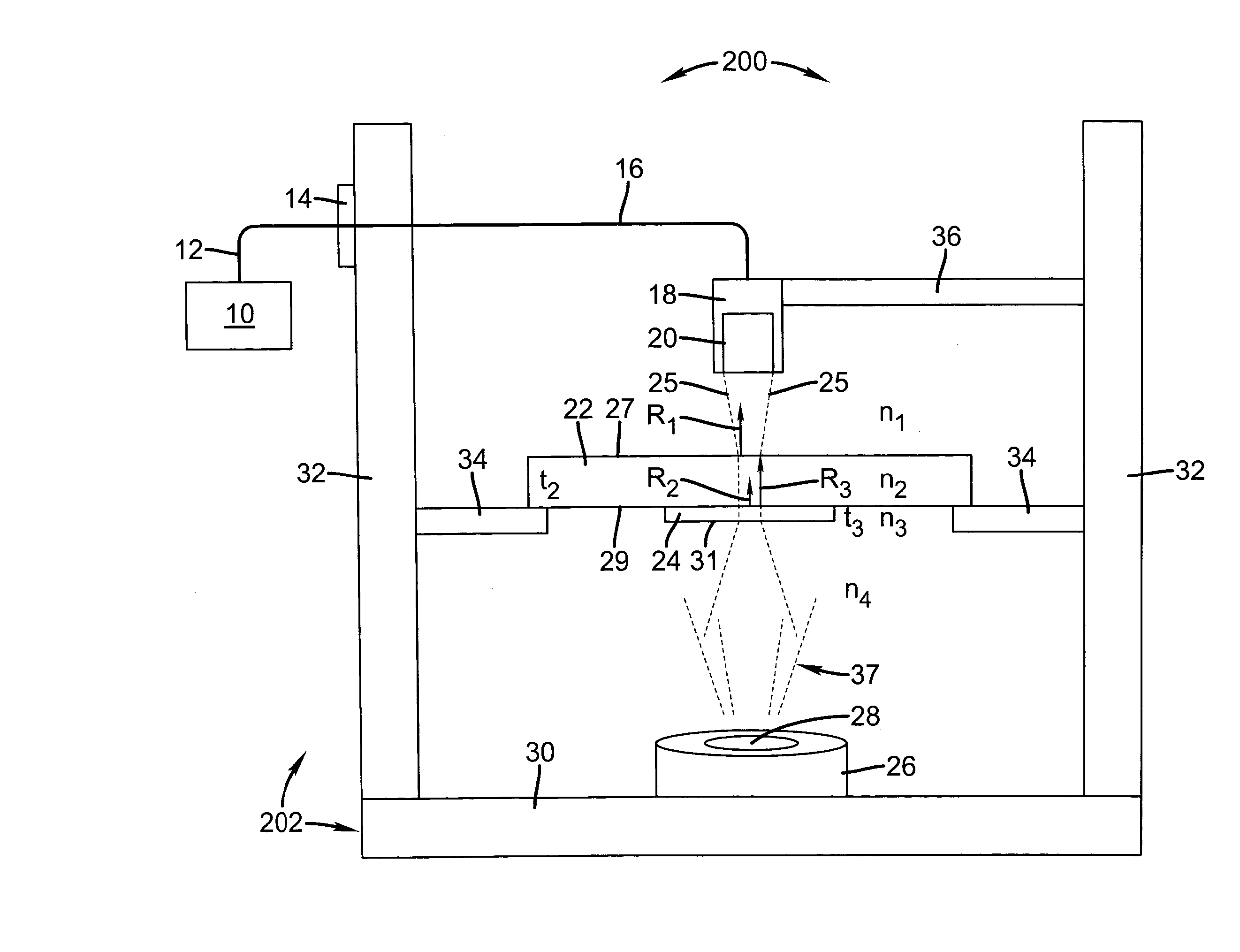
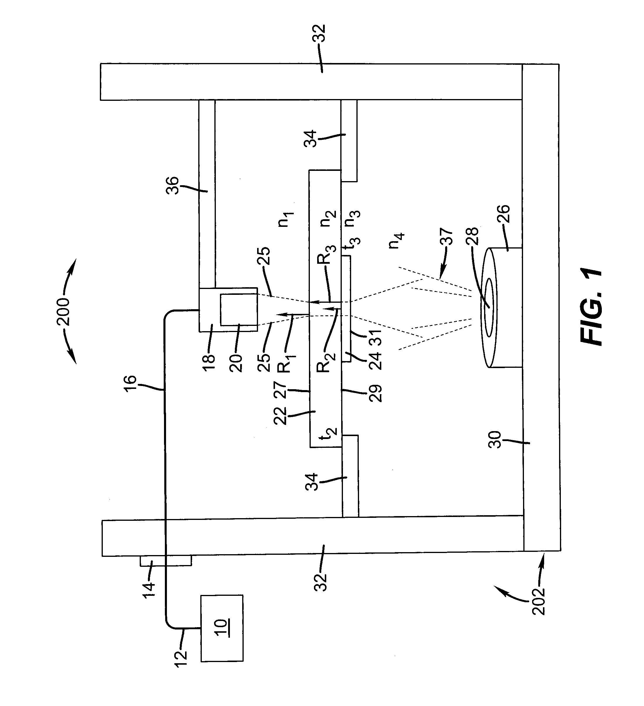
[0020] It is an advantage of the present invention that the total laydown thickness on an active device can be measured in-situ during coating, without the need of moving the sample to a separate measurement zone. Further, multilayered coatings can be measured in situ.
[0021] As a further advantage, the method of the present invention allows real-time monitoring of the deposition rate, useful in a control loop that regulates the laydown rate.
[0022] As a further advantage, the composition of a layer can also be determined when the layer consists of a host material and at least one dopant material.
[0023] As a further advantage, when using witness plates and masks, it is possible to employ built in reference materials.

Problems solved by technology

There are inherent difficulties that complicate the measurement process in the thin film deposition environment and that make some conventional approaches unworkable for in situ measurement.
Chief among these problems is the materials deposition process itself.
Thus, the performance of optical components and sensors will degrade over time due to deposition of material onto these control components.
This problem has been exhibited with so-called crystal mass-sensor devices, used in many thin-film development environments.
However, when the acceptable range of mass-loading of the crystal is exceeded, for example by build-up of an excess number of deposited layers, the oscillator circuit can no longer function reliably, necessitating replacement of the “overloaded” crystal with a new crystal mass-sensor.
Such replacement, in turn, requires discontinuation of the vapor deposition process.
In addition, when certain organic layers are deposited onto crystal mass-sensor devices there can be a tendency for the layers to start cracking and flaking from the mass sensor surface after coating thickness build-up on the order of 500-2,000 nanometer (nm).
This can cause the crystal mass-sensor to become inaccurate in its coating rate measurement capability at thicknesses well below the aforementioned mass-loading limit.
Thus, although the crystal mass-sensor device provides an acceptable solution for prototype and development work, this type of device, deteriorating with use and requiring regular replacement, would not be well suited for mass fabrication environments.
Lenses, photosensors, or other optical components that are exposed within the deposition chamber are all subject to this problem.
However, such a solution requires space in the deposition environment, requires an interface for its removal and reinsertion, introduces additional surface area and waste, and necessitates time delay so that the ability to obtain dynamic measurement data is compromised.
Although this method resolves a number of difficulties, however, it requires that the area to be measured be a surrogate area rather than the device being formed and that this measured area be moved out of the coating process to another position to be measured.
Although fluorescence may provide a suitable mechanism for measurement with some types of coatings, this method may have limited uses with other types of thin-film materials.
However, there is no acknowledgement of the problem of keeping the light source clean from contamination in this in situ arrangement or of maintaining equal power throughout the process.
For example, approaches such as those outlined in the Chow '6850 application and '1300 Atanasov application are not suited to in situ measurement.
The '4154 Masakuzu et al. application does not address the problem of contamination from deposited material.
More significantly, the methods described in the above-cited patent literature may perform adequately for single layer deposition, but do not work as well in measurement for components having multiple overlaid patterned layers.

Method used


Image

  • Measuring layer thickness or composition changes
  • Measuring layer thickness or composition changes
  • Measuring layer thickness or composition changes

Examples


example # 1

EXAMPLE #1

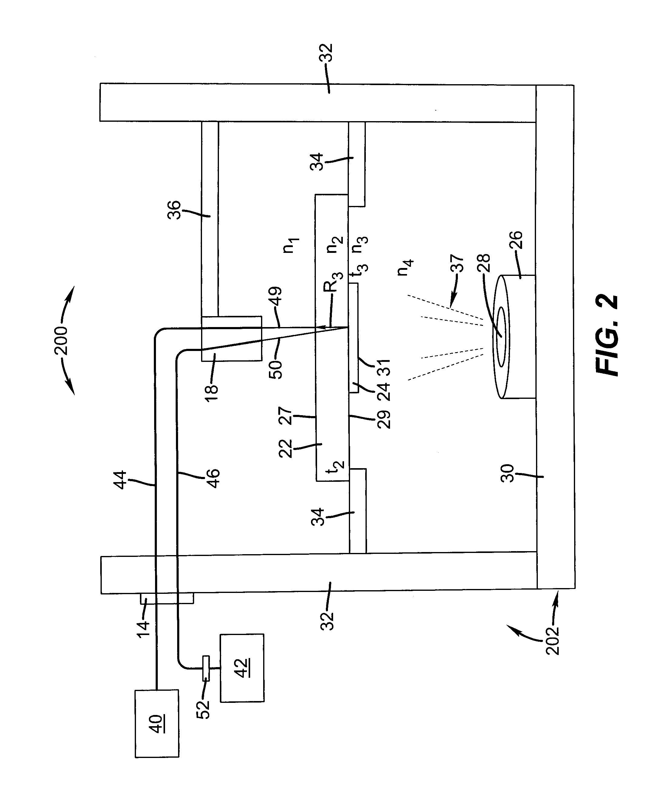
[0097] This example used a coating apparatus that operates at a pressure of about 1×10⁻⁶ Torr. The main working components designed for the in situ measurements are shown in FIG. 10. A witness plate 120, or mother glass or substrate, is disposed behind a metal aperture plate 126 or shadow mask that allows the plume of evaporated material to deposit a sample 122 through aperture 124 onto a known area, which is about a 1 inch diameter spot in the case of the metal plate. In one embodiment, the optics on excitation and collection fiber optic cables 44, 46 are collimating lenses, which illuminate and collect the luminescence from a spot of ¼″ radius. The excitation beam is collimated to ¼″, and collection fiber 46 also has a lens on it to view a ¼″ area overlapping with the excitation spot directed to sample 122. In one embodiment, collection fiber 46 is at approximately 22 degrees with respect to excitation fiber 44, and the plane containing collection and excitation fibers 4...


PUM


Abstract

A method of measuring the thickness or the rate of change of thickness of a layer as the layer is being formed on a substrate, includes illuminating the layer through the substrate with low coherence light that transmits through the layer; collecting a portion of the reflected light from each optical interface of the substrate and layer with a low coherence interferometer; and, calculating the thickness or the rate of change of thickness of the layer according to the obtained interferometric data.

Description

CROSS REFERENCE TO RELATED APPLICATION [0001] This application is a divisional of copending, commonly assigned U.S. patent application Ser. No. 11 / 262,868 filed Oct. 31, 2005.FIELD OF THE INVENTION [0002] The present invention relates to providing physical measurements of layer thickness and more particularly relates to measuring the thickness of a layer of material during or after it is deposited on a substrate and also relates to determining the relative concentration of a deposited component of the layer during or after deposition. BACKGROUND OF THE INVENTION [0003] Many types of optical and electro-optical elements require the deposition of at least one, but typically multiple patterned thin film coatings onto a substrate. In order to obtain the optimum performance from these optical and electro-optical elements and to achieve satisfactory fabrication yields, it is necessary to provide precise control over the materials deposition process. One key aspect of this control relates ...

Claims


Application Information

Patent Timeline
Patent Type & Authority Applications(United States)
IPC IPC(8): G01B11/06
CPCH01L22/12G01B11/0683
Inventor MARCUS, MICHAEL A.SWITALSKI, STEVEN C.
Owner GLOBAL OLED TECH
Learn More