Method of plasma etching with pattern mask

Inactive Publication Date: 2007-11-15
ADVANCED CHIP ENG TECH
View PDF2 Cites 5 Cited by
  • Summary
  • Abstract
  • Description
  • Claims
  • Application Information

AI Technical Summary

Benefits of technology

[0006] Besides, another advantage of the present invention is that the present invention provides a dry etching system with a mask attaching module which is inexpensive than PR coating module. Besides, the PR coating process, including hard bake for drying the water, therefore it takes more time for conventional PR process.
[0007] The present invention may be applied to the removal of layer, material formed on an area of signal die. Furthermore, the material under removing is not limited to oxide, any undesired material could be removed by the present invention. For example, the present invention can be applied to remove unwanted coating on a CMOS sensor.
[0008] The main purpose of the present invention is to provide a method of etching, comprises: providing a mask having a buffer film formed thereon, wherein the mask has at least one air opening formed through the mask to the buffer later; attaching the mask on a wafer through the buffer film to cover a portion of the wafer to allow the at least one air opening expose an area to be etched, wherein the wafer including a silicon based area and a GaAs based area, and the wafer includes a die having at least one area under etching; the material of the buffer film includes elastic material, for instance, silicone resin, elastic PU, porous PU, acrylic rubber, blue tape, UV tape, polyimide (PI), polyester (PET), or polypropyl

Problems solved by technology

Besides, the PR coating process, including hard bake for drying th

Method used


Image

  • Method of plasma etching with pattern mask
  • Method of plasma etching with pattern mask
  • Method of plasma etching with pattern mask

Examples


Example

[0015] Some sample embodiments of the invention will now be described in greater detail. Nevertheless, it should be recognized that the present invention can be practiced in a wide range of other embodiments besides those explicitly described, and the scope of the present invention is expressly not limited expect as specified in the accompanying claims. Then, the components of the different elements are not shown to scale. Some dimensions of the related components are exaggerated and meaningless portions are not drawn to provide clearer description and comprehension of the present invention.

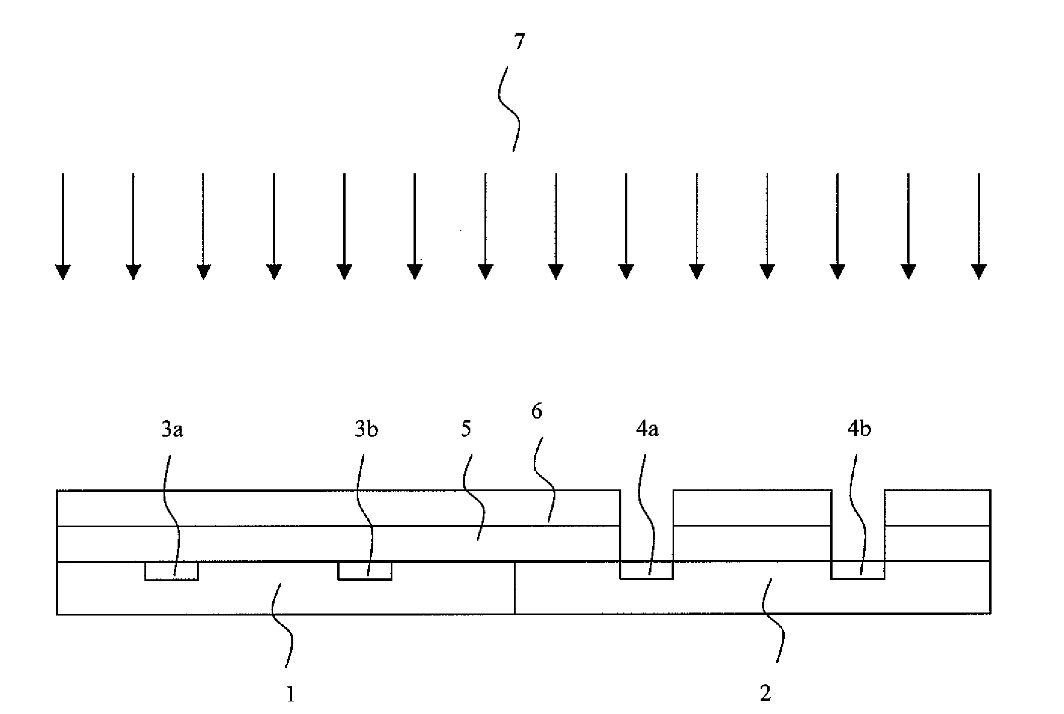
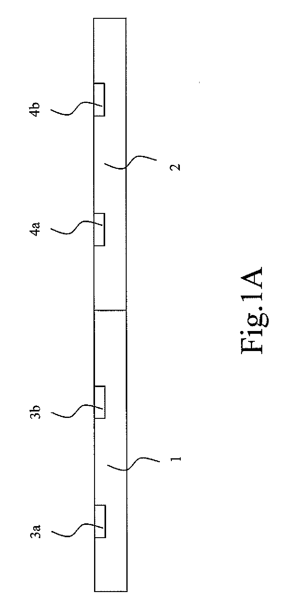
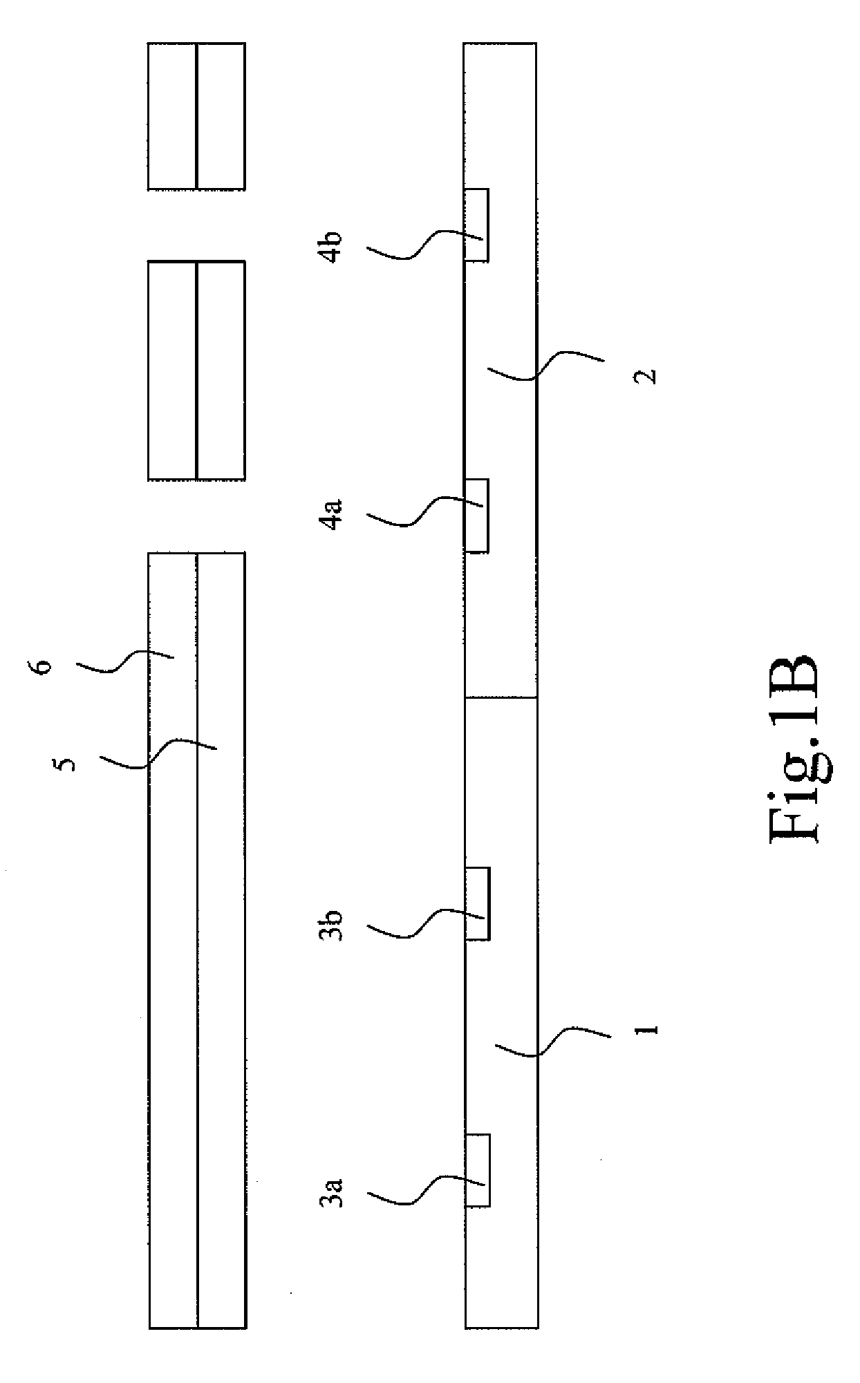
[0016] The present invention discloses a method for plasma etching. Serial steps of the method are shown in FIG. 1A to FIG. 1D separately. First, a wafer including at least two different areas 1 and 2 on the wafer is provided as shown in FIG. 1A, the materials of the areas 1 and 2 maybe silicon and Gallium Arsenide (GaAs), respectively. The areas 1 and 2 are used for forming two different specie...


PUM

PropertyMeasurementUnit
Areaaaaaaaaaaa
Elasticityaaaaaaaaaa
Semiconductor propertiesaaaaaaaaaa

Abstract

The present invention provides a method of plasma etching with pattern mask. There are two different devices in the two section of a wafer, comprising silicon and Gallium Arsenide (GaAs). The Silicon section is for general semiconductor. And the GaAs section is for RF device. The material of pad in the silicon is usually metal, and metal oxide is usually formed on the pads. The metal oxide is unwanted for further process; therefore it should be removed by plasma etching process. A film is attached to the surface of the substrate exposing the area need for etching. Then a mask is attached and aligned onto the film therefore exposing the area need for etching. Then plasma dry etching is applied on the substrate for removing the metal oxide.

Description

FIELD OF THE INVENTION [0001] This invention relates to an etching method for package assembly, and particularly, to a method of plasma etching with a pattern mask. BACKGROUND OF THE INVENTION Description of the Prior Art [0002] In the process and manufacture of semiconductor, it is necessary to etch the thin films previously deposited and / or the substrate itself. In general, there are two classes of etching processes, that is: wet etching and dry etching. Wet etching is to dissolve the material when immersed in a chemical solution, while dry is to sputter or dissolve etching the material using reactive ions or plasma. A disadvantage of wet etching is the undercutting caused by the isotropy of etch. The purpose of dry etching is to create an anisotropic etch—meaning that the etching is uni-directional. An anisotropic etch is critical for high-fidelity pattern transfer. [0003] The fluorine ions are accelerated in the electric field causing them to collide into the surface of the samp...

Claims


Application Information

Patent Timeline
IPC IPC(8): C03C25/68C23F1/00H01L21/306
CPCH01L21/321H01L21/31144H01L21/306H01L21/3065
Inventor YANG, WEN-KUNCHANG, JUI-HSIENSUN, WEN-BIN
Owner ADVANCED CHIP ENG TECH
Why Eureka
Try Eureka