

Formation of carbon and semiconductor nanomaterials using molecular assemblies
a technology of molecular assemblies and nanomaterials, which is applied in the direction of nanoinformatics, crystal growth process, polycrystalline material growth, etc., can solve the problems of limited success in the formation of electrical devices using carbon nanotubes, small portion of individual nanotubes actually coming into contact with electrodes, and nanostructures to potentially harmful conditions, etc., to achieve the effect of increasing the amount of metal on the surfa
- Summary
- Abstract
- Description
- Claims
- Application Information
AI Technical Summary
Benefits of technology
Problems solved by technology
Method used
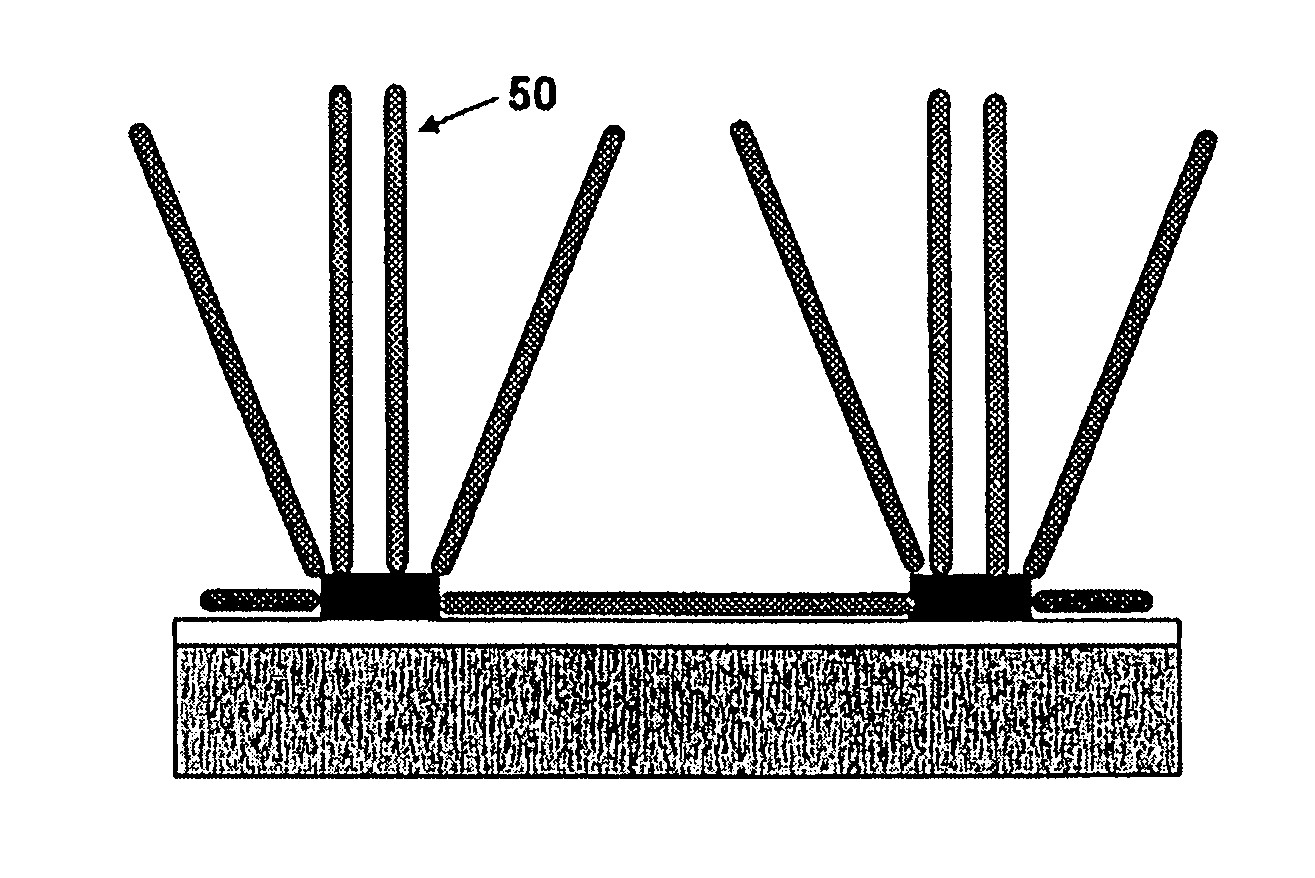
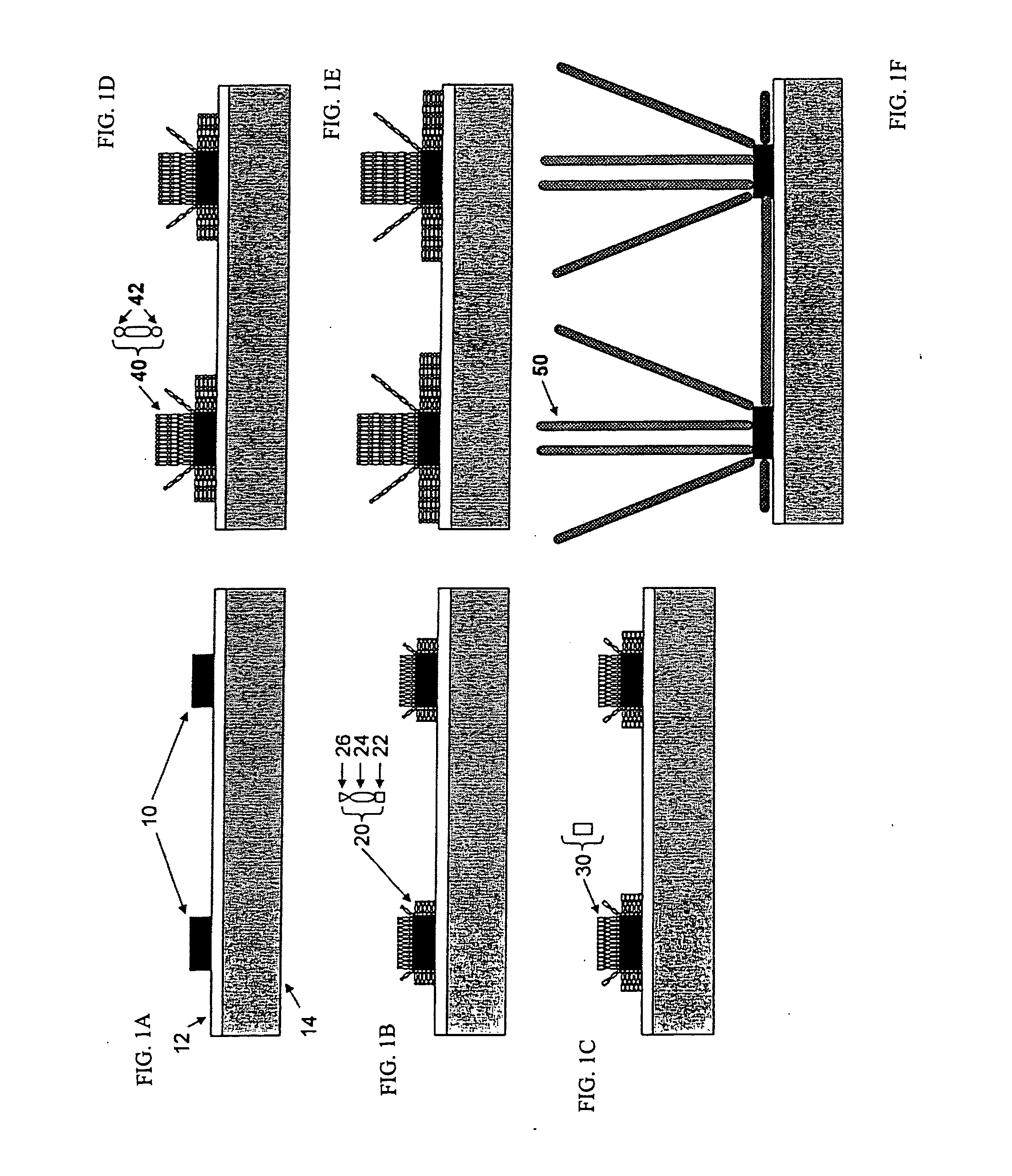
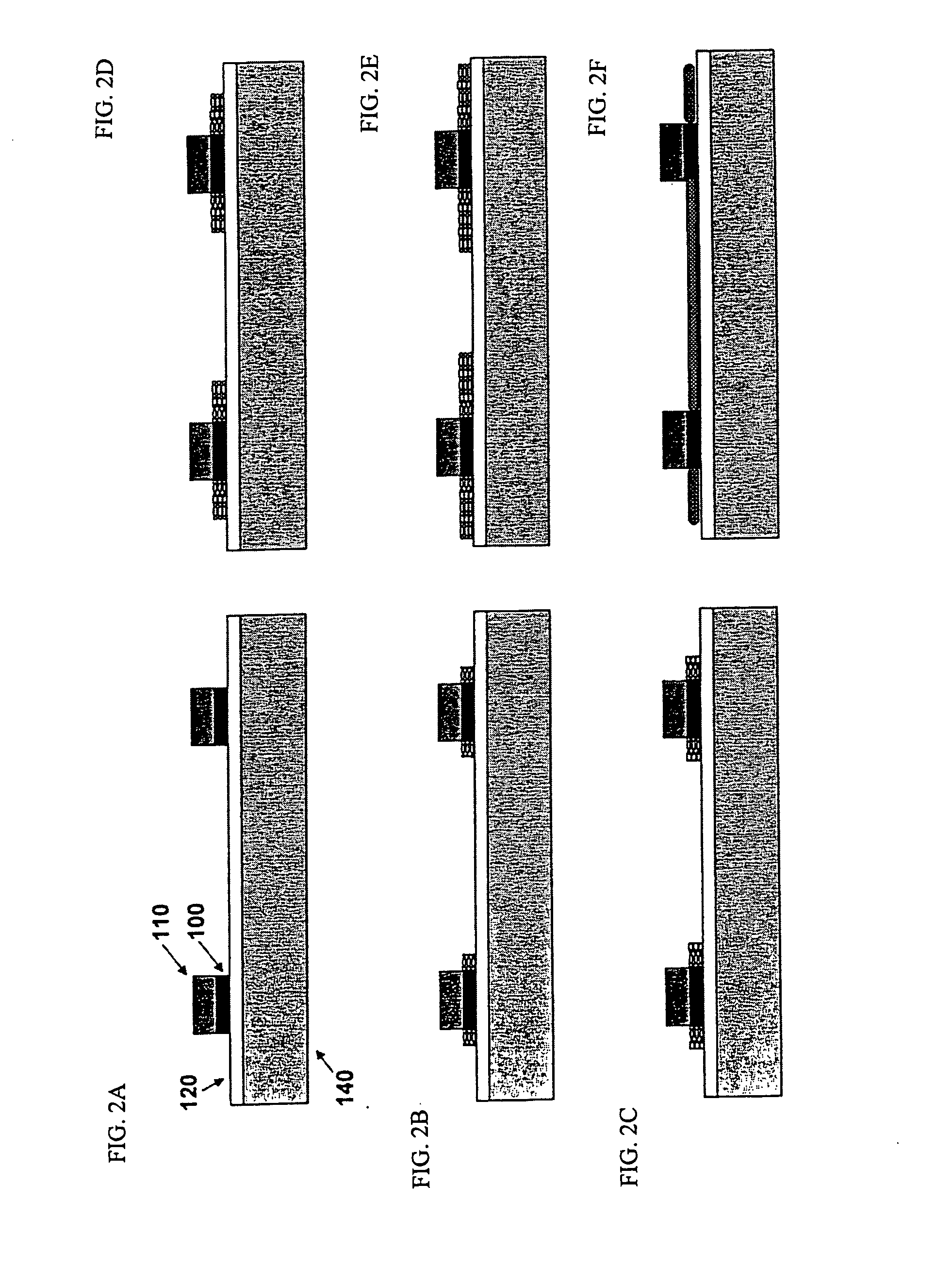
Image

Examples
example 1
[0078] A heavily n+ doped silicon wafer, with 10 nm thermally grown silicon oxide was patterned with electrodes consisting of 10 Å Ti followed by 190 Å Pd. The patterned substrate was exposed to 1 mM mercaptoterypyridine in 50:50 toluene:ethanol for a period of 18 hrs, resulting in the assembly of mercaptoterypridine on the Pd surfaces. The samples were rinsed well in clean 50:50 toluene:ethanol and exposed to 5 mM FeCl3 in ethanol for a similar period of 18 hrs. The samples were rinsed in clean ethanol and dried under a nitrogen stream.
example 2
[0079] A heavily n+ doped silicon wafer, with 10 nm thermally grown silicon oxide was patterned with electrodes consisting of 10 Å Ti followed by 190 Å Pd. The patterned substrate was exposed to 1 mM mercaptoterypyridine in 50:50 toluene:ethanol for a period of 18 hrs, resulting in the assembly of mercaptoterypridine on the Pd surfaces. The samples were rinsed well in clean 50:50 toluene:ethanol and exposed to dispersion of iron oxide nanoparticles in hexane for a period of 18 hrs. The samples were rinsed in clean hexane and dried under a nitrogen stream.
example 3
[0080] A heavily n+ doped silicon wafer, with 10 nm thermally grown silicon oxide was patterned with electrodes consisting of 10 Å Ti followed by 190 Å Pd. The patterned substrate was exposed to 1 mM aminoethanethiol in ethanol for 18 hrs, resulting in the assembly of aminoethanethiol on the Pd surfaces. The samples were rinsed well with clean ethanol and exposed to a dispersion of iron oxide nanoparticles in hexane for a period of 18 hrs. The samples were rinsed in clean hexane and dried under a nitrogen stream.
PUM
| Property | Measurement | Unit |
|---|---|---|
| semiconductor | aaaaa | aaaaa |
| photosensitive | aaaaa | aaaaa |
| semiconducting | aaaaa | aaaaa |
Abstract
Description
Claims
Application Information