Resistive memory device

a memory cell and resistive technology, applied in the direction of negative resistance effect devices, semiconductor devices, bulk negative resistance devices, etc., can solve the problems of increasing the limits of conventional electronic data memories, such as dynamic random access memory (dram) or flash memory, to meet modern requirements, require substantial energy, and provide limited endurance, so as to improve the method of fabricating a programmable resistive memory cell. , the effect of improving the programmable resistive memory cell

Inactive Publication Date: 2007-11-22
INFINEON TECH AG
View PDF6 Cites 44 Cited by
  • Summary
  • Abstract
  • Description
  • Claims
  • Application Information

AI Technical Summary

Benefits of technology

[0012]The present invention provides advantages for an improved programmable resistive memory cell, and an improved method of fabricating a programmable resistive memory cell.

Problems solved by technology

Conventional electronic data memories, for example dynamic random access memory (DRAM) or flash RAM, increasingly run into limits when they are to meet modern requirements.
Besides additional memory controllers for refreshing, this also requires substantial energy.
On the other hand, the flash RAM retains the stored information content without external power being supplied, but the individual flash RAM memory cells require high voltages for writing information and provide a limited endurance only.
The requirements with respect to information density and non-volatility become apparent also in portable applications, since the available space is limited and the batteries, serving as a power supply, are only able to provide limited energy and voltages.
The minimum size of such a TMO memory cell is primarily given by lithographic limitations with respect to the patterning of the electrodes.
However, initial programming with a high voltage is usually necessary.
However, the high initial programming voltages are in conflict with the integration of TMO storage cells.
The application of a voltage in the range of the breakdown voltage may adversely alter the memory cell or may also result in a complete failure thereof after only a few switching cycles.
However, problems arise as far as the manufacturing and the operation of oxygen-deficient transition metal oxides are concerned: The controlled and well-defined deposition of oxygen-deficient transition metal oxides is difficult to achieve with a satisfactory degree of reproducibility.

Method used


Image

  • Resistive memory device
  • Resistive memory device
  • Resistive memory device

Examples


first embodiment

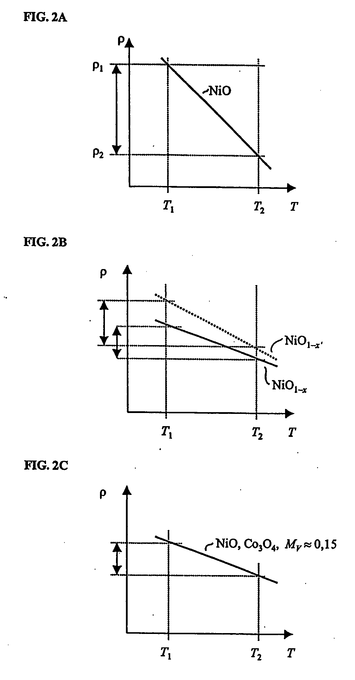
[0028]FIG. 2C shows a schematic plot of the temperature-dependent resistance of a combination of two transition metal oxides, for example, nickel oxide and cobalt oxide, according to the present invention. Therein, a programmable resistance layer comprises two transition metal oxides, TMO1 and TMO2, in an atomic / molecular ratio

MR=TMO1 / (TMO1+TMO2),   (2)

wherein TMO1 and TMO2 denote the respective atomic content of the first and second transition metal oxide. The ratio MR, as defined by (2), may determine both the initial electrical resistance and the temperature-dependence of the electrical resistance of the combined oxide layer. The ratio MR may be set reliably and reproducibly during deposition, for example, during sputtering, by varying the corresponding sputtering rates. In addition, the ratio MR may then be stably maintained in the programmable resistance layer even without the need for diffusion barriers or other measures. Using corresponding transition metal oxides, both the i...

second embodiment

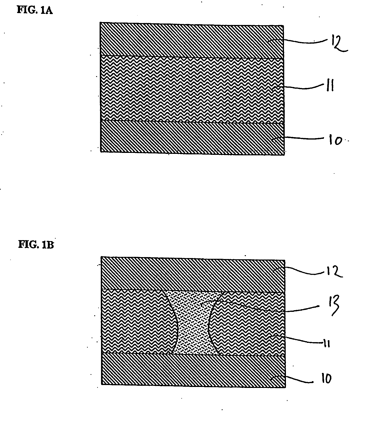
[0029]FIGS. 3A through 3C show a schematic view of a resistive memory cell in different stages during fabrication according to the present invention. As shown in FIG. 3A, first, a lower electrode 10 is provided. As shown in FIG. 3B, a programmable resistive layer 11 is provided on the lower electrode 10, for example, by means of reactive co-sputtering. During sputtering, a DC, MF or RF plasma excitation may be effected, in order to sputter a solid element or oxide target. Therein, at least two transition metals, a first transition metal 101 and a second transition metal 102, are sputtered. In the case of sputtering elementary transition metals, the process atmosphere during formation of the programmable resistance layer 11 comprises oxygen 100 for forming the corresponding oxides 110, 120. As shown, the process atmosphere comprises at least so much oxygen 100 that the sputtered transition metals 101 and 102 may oxidize in their respective highest degree of oxidation and thus form a ...

third embodiment

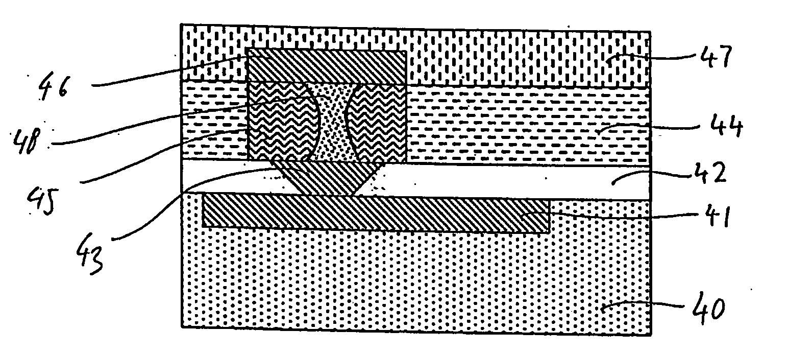
[0032]FIGS. 4A through 4H show a schematic view of a resistive memory cell in different stages during fabrication according to the present invention. First, as shown in FIG. 4A, a substrate 40 is provided. As shown in FIG. 4B, a trench 400 is formed in the substrate 40. The substrate 40 may include a silicon substrate or other already structured functional elements—as is usual in semiconductor manufacturing. The trench 400 in the substrate 40 serves for forming a lower electrode 41, as shown in FIG. 4C. In the case of a insulating or semi-insulating substrate 40, a plurality of lower electrodes 41 or also conductive tracks may be arranged side-by-side for contacting a plurality of resistive memory cells, wherein the contacts or tracks are electrically isolated from each other.

[0033]The surface of the lower electrode 41 and of the substrate 40 may be polished, e. g. by means of chemical mechanical polishing, for the provision of a planar surface for the following process stages.

[0034...


PUM


Abstract

A programmable resistive memory cell comprising a lower electrode, a programmable resistance layer, and an upper electrode, wherein the programmable resistance layer comprises a first transition metal oxide and a second transition metal oxide.

Description

TECHNICAL FIELD OF THE INVENTION[0001]The invention relates to a programmable resistive memory cell with a programmable resistance layer and to a method of fabricating a resistive memory cell with a programmable resistance layer.BACKGROUND OF THE INVENTION[0002]Conventional electronic data memories, for example dynamic random access memory (DRAM) or flash RAM, increasingly run into limits when they are to meet modern requirements. Conventional concepts for electronic data memories, as are also employed in the case of DRAM and flash RAM, store information units in capacitors, wherein a charged or an uncharged state of the capacitor represent, for instance, the two logic states “1” or “0”.[0003]In case of the DRAM, the capacitors are designed extremely small in order to achieve high information density and integration, and thus require constant refreshing of the stored information content. Besides additional memory controllers for refreshing, this also requires substantial energy. On ...

Claims


Application Information

Patent Timeline
Patent Type & Authority Applications(United States)
IPC IPC(8): H01L47/00
CPCH01L27/2436H01L27/2472H01L45/085H01L45/1273H01L45/146H01L45/1625H01L45/1683H01L45/1233H10B63/82H10B63/30H10N70/245H10N70/8418H10N70/826H10N70/8833H10N70/026H10N70/066
Inventor UFERT, KLAUS DIETER
Owner INFINEON TECH AG
Why Eureka
Try Eureka