Printed wiring board, method for forming the printed wiring board, and board interconnection structure

a technology of printed wiring and interconnection structure, which is applied in the manufacture of printed circuits, printed circuit aspects, basic electric elements, etc., can solve the problems of reducing the miniaturization and weight of connector parts, affecting the miniaturization and weight reduction, and the cost of connector parts is added to the total cost in the case of multi-signal connection, so as to reduce the peeling strength and enhance the connection strength

Inactive Publication Date: 2007-11-29
THE FUJIKURA CABLE WORKS LTD
View PDF99 Cites 17 Cited by
  • Summary
  • Abstract
  • Description
  • Claims
  • Application Information

AI Technical Summary

Benefits of technology

[0018] According to the present invention, the decrease of the peeling strength between the connection terminals and the insulating layer, and the solder bridges (short circuit) between the connection terminals, owing to excessive solder, can be prevented without inhibiti

Problems solved by technology

However, if the function of the electronic instrument becomes higher, types of the electric signals between the boards are also increased, and the above-described connecting space is increased, which lead to inhibit such miniaturization and weight reduction.
However, it is difficult to miniaturize the connector parts having fitting mechanisms.
Moreover, in the connector parts, electric bonding is performed therefor by compressively bonding terminals to each other, and accordingly, the connector parts are inferior in bonding themselves is generated, and accordingly, expense of the connector parts is added to total cost in the case of multi-signal connection.
Since, however, microfabrication and pitch fining of the conductive circuits of the printed wiring boards are advanced in recent years, problems occur in the connection method as described above.
Therefore, there is an apprehension that the solder that has squeezed out may be brought into contact with the solder on the adjacen

Method used


Image

  • Printed wiring board, method for forming the printed wiring board, and board interconnection structure
  • Printed wiring board, method for forming the printed wiring board, and board interconnection structure
  • Printed wiring board, method for forming the printed wiring board, and board interconnection structure

Examples


first non-limiting embodiment

(Printed Wiring Board)

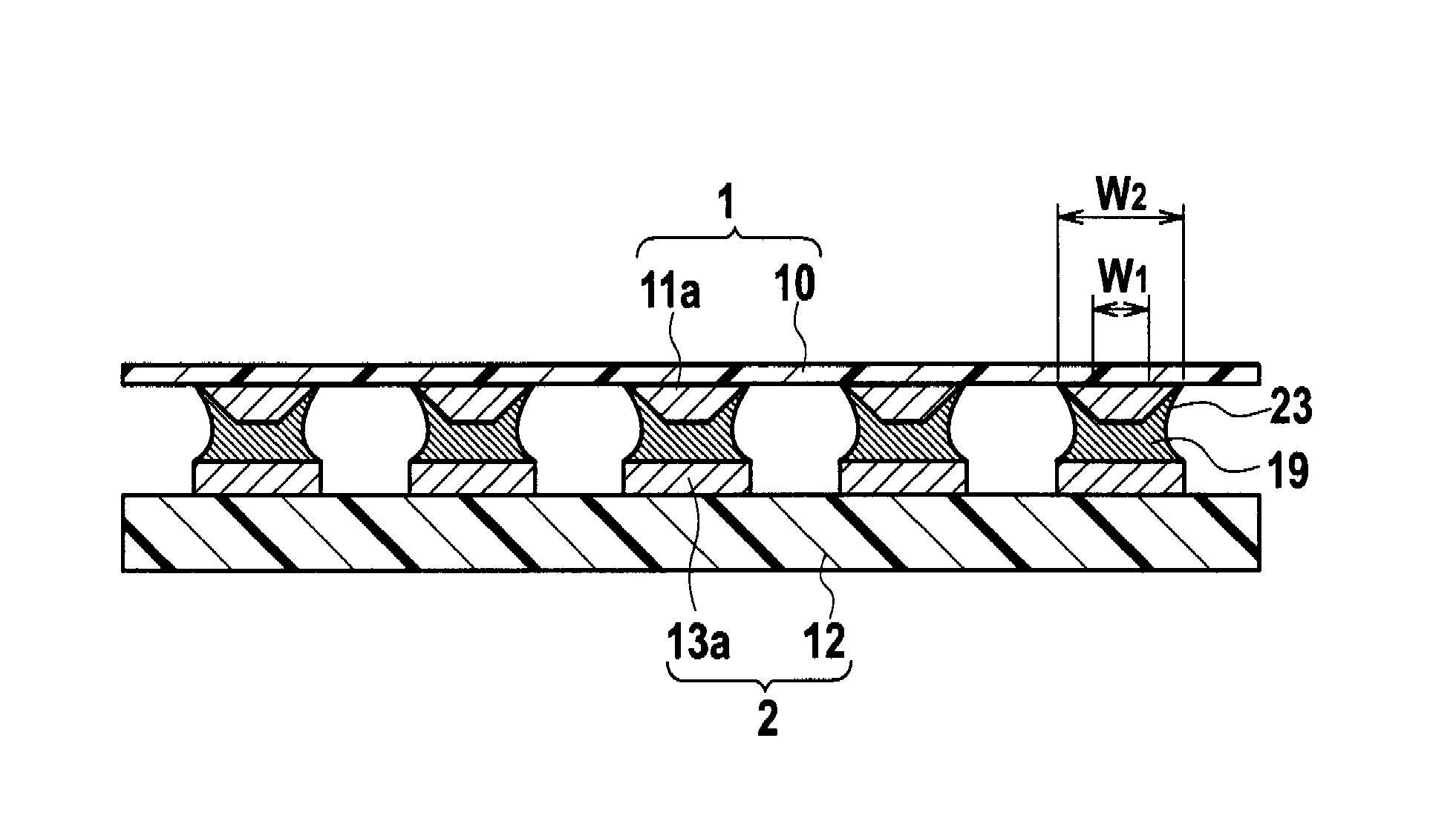
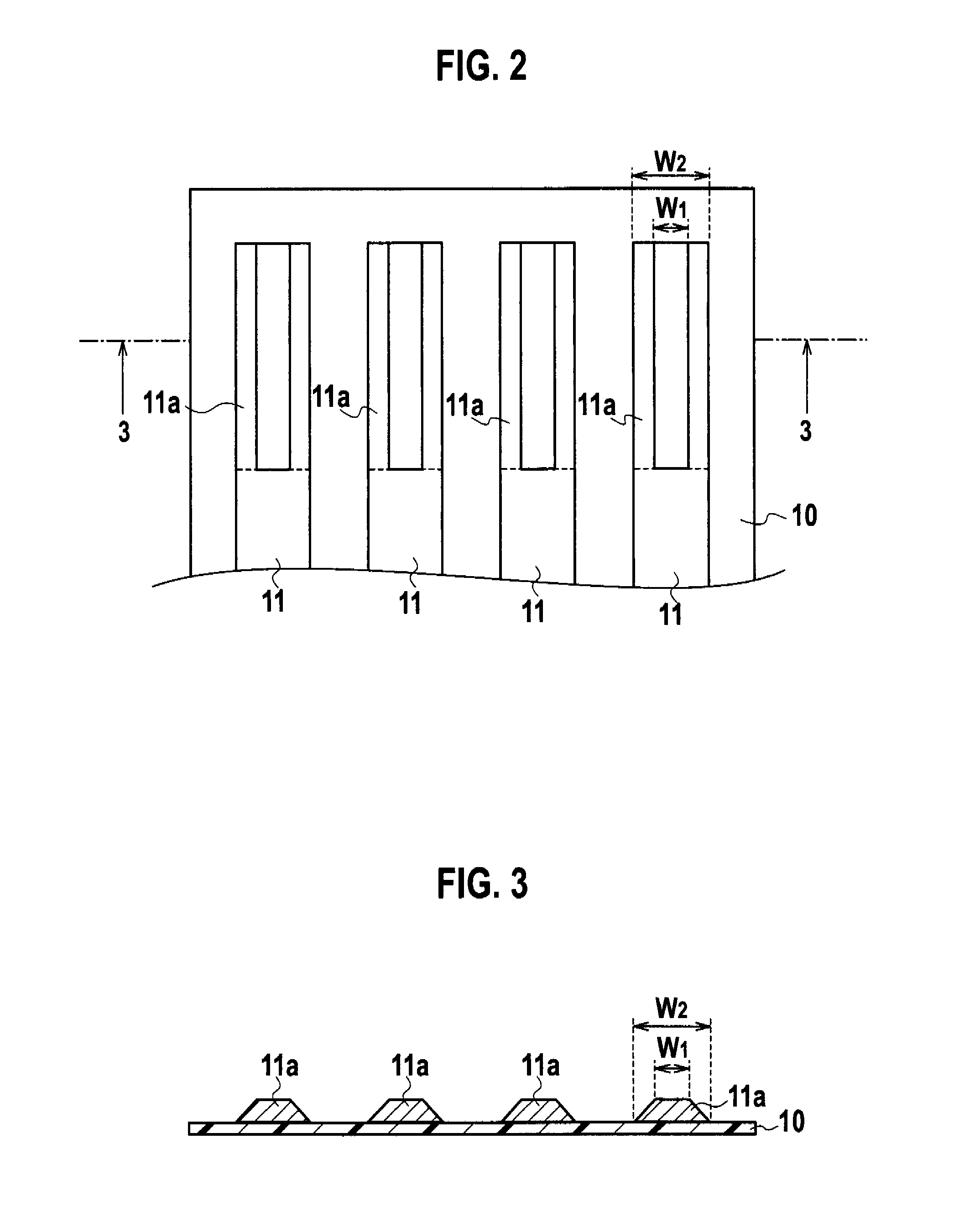
[0035] As shown in FIG. 2, a printed wiring board according to a first embodiment of the present invention includes an insulating layer 10, and conductive circuits 11 having, on end portions thereof, connection terminals 11a in each of which a width W1 of an upper surface is narrower than a width W2 of a bottom surface. FIG. 3 is a cross-sectional view of the printed wiring board viewed from a direction of a line 3-3 of FIG. 3.

[0036] As the insulating layer 10, for example, a flexible board such as a polyimide board, a polyethylene terephthalate (PET) board, and a polyethylene naphthalate (PEN) board can be used. Alternatively, as the insulating layer 10, for example, a hard rigid board such as a glass epoxy board, a glass composite board, and a paper epoxy board can be used. It is preferable that the insulating layer 10 have heat resistance to a temperature of a melting point of a solder or higher. In the case of using the rigid board as the insulating laye...

second non-limiting embodiment

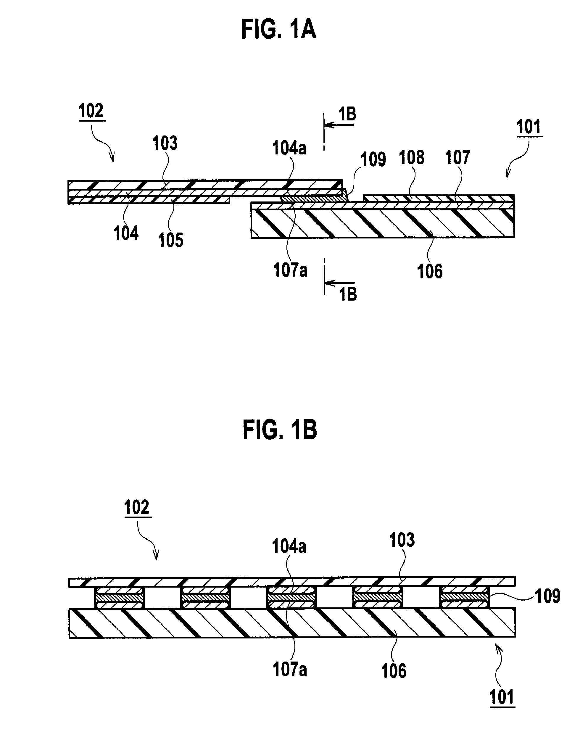
[0051] As shown in FIG. 5, a board interconnection structure according to a second embodiment of the present invention is different from that of FIG. 4, in the case of comparison therebetween, in that an upper surface width W3 of the connection terminals 13b is more narrow than a bottom surface width W4 of the connection terminals 13b of a second printed wiring board 2a. Other elements shown in FIG. 5 are substantially similar to those in the board interconnection structure shown in FIG. 4, and accordingly, a duplicate description will be omitted.

[0052] In accordance with the board interconnection structure according to the second embodiment, connection areas between the first insulating layer 10 and the first connection terminals 11a and between the second insulating layer 12 and the second connection terminals 13b are not reduced. Hence, the connection strengths between the first insulating layer 10 and the first connection terminals 11a and between the second insulating layer 12...

third non-limiting embodiment

(Printed Wiring Board)

[0056] As shown in FIG. 6, a printed wiring board according to a third embodiment of the present invention includes an insulating layer 10, conductive circuits 14 arranged on the insulating layer 10 and having connection terminals 15 on end portions thereof, and projection portions 16 provided on the connection terminals 15 in a direction where the conductive circuits 14 are extended. FIG. 7 is a cross-sectional view of the printed wiring board viewed from a direction of a line 7-7 of FIG. 6.

[0057] The insulating layer 10 is similar to that of the first embodiment.

[0058] The conductive circuits 14 form a circuit pattern of conductors, which are designed on the insulating layer 10. In the case of the pattern formation using the subtractive method, the conductive circuits 14 are formed by etching the rolled copper foil, the electrolytic copper foil, or the like on the insulating layer 10. Other metal foil than the copper foil is also usable as the conductors....


PUM


Abstract

A board interconnection structure having a first printed wiring board in which a first conductive circuit is arranged on a first insulating layer, the first conductive circuit having, on an end portion thereof, a first connection terminal in which an upper surface width is narrower than a bottom surface width; a second printed wiring board in which a second conductive layer having a second connection terminal is arranged on a second insulating layer; and a connection layer that forms fillets along longitudinal side surfaces of the first connection terminal, and interconnects the first connection terminal and the second connection terminal. The first connection terminal may have a projection portion.

Description

[0001] Priority is claimed from Japanese Patent Application No. 2006-145389 and 2006-145390, filed May 25, 2006, the contents of which are incorporated herein by reference. BACKGROUND [0002] The present invention relates to a technology for interconnecting printed boards. In particular, the present invention relates to a printed wiring board, a method for forming the printed wiring board, and a board interconnection structure, which enhances interconnection strength of the boards. DESCRIPTION OF THE RELATED ART [0003] As an electronic instrument is being required to be smaller, lighter in weight, and higher in function, it is more necessary to install a plurality of boards three-dimensionally in a small space of the product. For this, a space for connecting electric signals between the boards must be reduced. However, if the function of the electronic instrument becomes higher, types of the electric signals between the boards are also increased, and the above-described connecting sp...

Claims


Application Information

Patent Timeline
IPC IPC(8): H01L23/48H01L21/00
CPCH05K3/363H05K2201/09745H05K2201/098H05K2201/09845H01L2924/0002H01L2924/00H05K1/02
Inventor KITADA, TOMOFUMIMARUO, HIROKITAKAMI, RYO
Owner THE FUJIKURA CABLE WORKS LTD
Why Eureka
Try Eureka