Functional Materials and Novel Methods for the Fabrication of Microfluidic Devices

a microfluidic device and functional material technology, applied in the field of functional materials, can solve the problems of microfluidic drawbacks, high cost and labor intensity of photolithography and etching techniques, and require clean-room conditions, and achieve the effect of rapid catalyst screening and enzyme-protein interaction screening

Inactive Publication Date: 2007-11-29
THE UNIV OF NORTH CAROLINA AT CHAPEL HILL
View PDF99 Cites 224 Cited by
  • Summary
  • Abstract
  • Description
  • Claims
  • Application Information

AI Technical Summary

Benefits of technology

[0063] Further, the presently disclosed subject matter provides functional materials for use in attaching biological and other “switchable” molecules to the interior surface of a microfluidic channel. For example, attaching a biomolecule, such as a biopolymer, to the interior surface of a microfluidic channel, provides for combinatorial peptide synthesis and / or rapid screening of enzyme-protein interactions. Further, lining a microfluidic channel with a catalyst, allows for rapid catalyst screening. Also, introduction of a switchable organic molecule into a microfluidic channel allows for the fabrication of microfluidic devices comprising hydrophilic channels and hydrophobic channels.

Problems solved by technology

Photolithography and etching techniques, however, are costly and labor intensive, require clean-room conditions, and pose several disadvantages from a materials standpoint.
The increasing complexity of microfluidic devices has created a demand to use such devices in a rapidly growing number of applications.
Despite the aforementioned advantages, PDMS suffers from a drawback in microfluidic applications in that it swells in most organic solvents.
Thus, PDMS-based microfluidic devices have a limited compatibility with various organic solvents.
The swelling of a PDMS microfluidic device by organic solvents can disrupt its micron-scale features, e.g., a channel or plurality of channels, and can restrict or completely shut off the flow of organic solvents through the channels.
Thus, microfluidic applications with a PDMS-based device are limited to the use of fluids, such as water, that do not swell PDMS.
This approach, however, is limited by the disadvantages of fabricating microfluidic devices from hard materials.
Moreover, PDMS-based devices and materials are notorious for not being adequately inert enough to allow them to be used even in aqueous-based chemistries.
For example, PDMS is susceptible to reaction with weak and strong acids and bases.
PDMS-based devices also are notorious for containing extractables, in particular extractable oligomers and cyclic siloxanes, especially after exposure to acids and bases.

Method used


Image

  • Functional Materials and Novel Methods for the Fabrication of Microfluidic Devices
  • Functional Materials and Novel Methods for the Fabrication of Microfluidic Devices
  • Functional Materials and Novel Methods for the Fabrication of Microfluidic Devices

Examples


example 1

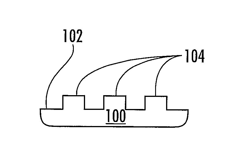
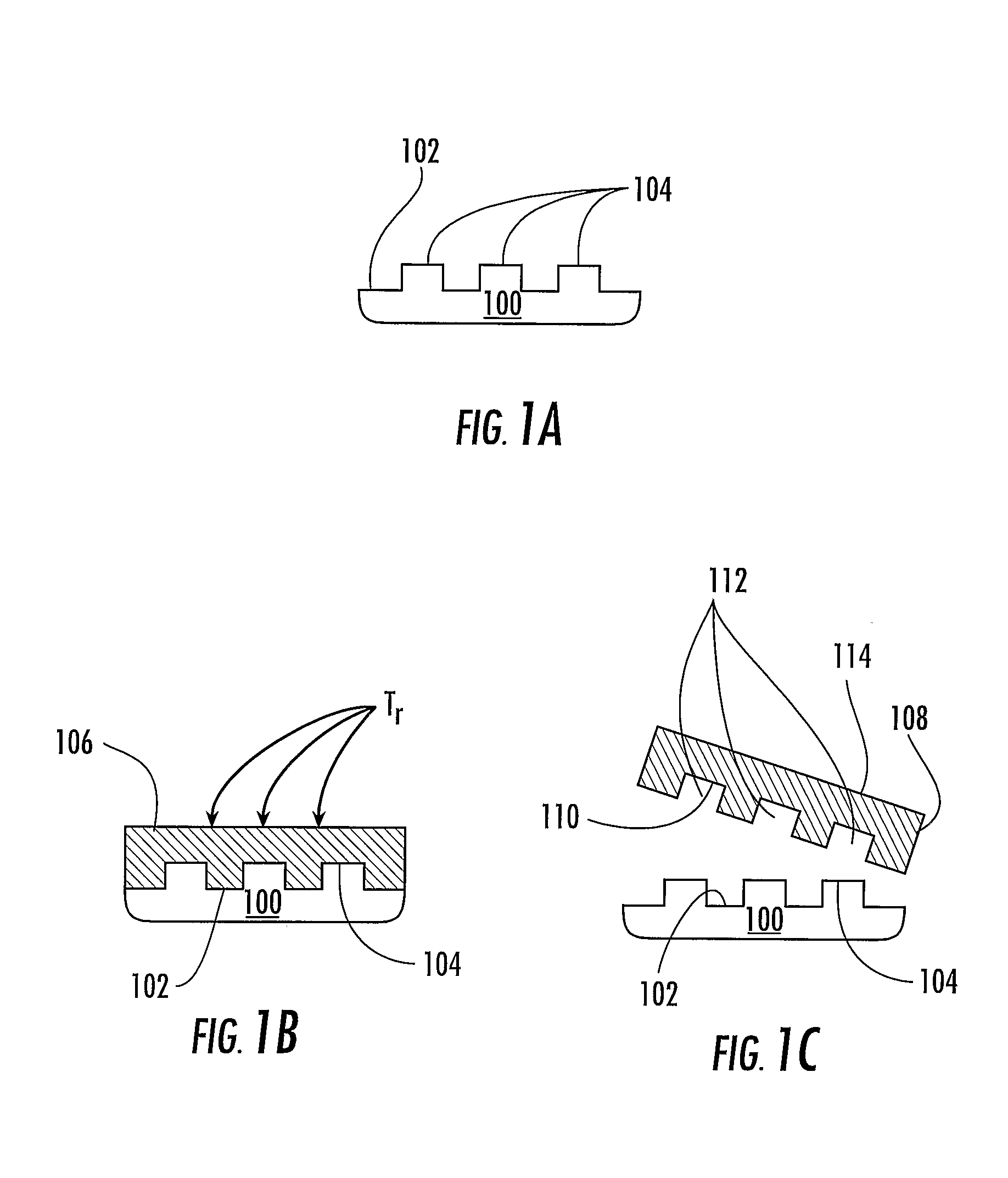
[0371] A liquid PFPE precursor having the structure shown below (where n=2) is blended with 1 wt % of a free radical photoinitiator and poured over a microfluidics master containing 100-μm features in the shape of channels. A PDMS mold is used to contain the liquid in the desired area to a thickness of about 3 mm. The wafer is then placed in a UV chamber and exposed to UV light (λ=365) for 10 minutes under a nitrogen purge. Separately, a second master containing 100-μm features in the shape of channels is spin coated with a small drop of the liquid PFPE precursor over top of it at 3700 rpm for 1 minute to a thickness of about 20 μm. The wafer is then placed in a UV chamber and exposed to UV light (λ=365) for 10 minutes under a nitrogen purge. Thirdly, a smooth, flat PFPE layer is generated by drawing a doctor's blade across a small drop of the liquid PFPE precursor across a glass slide. The Slide is then placed in a UV chamber and exposed to UV light (λ=365) for 10 minutes under a n...

example 2

Thermal Free Radical Glass

[0372] A liquid PFPE precursor encapped with methacrylate groups is blended with 1 wt % of 2,2-Azobisisobutyronitrile and poured over a microfluidics master containing 100-μm features in the shape of channels. A PDMS mold is used to contain the liquid in the desired area to a thickness of about 3 mm. The wafer is then placed in an oven at 65° C. for 20 hours under nitrogen purge. The cured layer is then removed, trimmed, and inlet holes are punched through it using a luer stub. The layer is then placed on top of a clean glass slide and fluids are introduced through the inlet holes.

example 3

Thermal Free Radical—Partial Cure Layer to Layer Adhesion

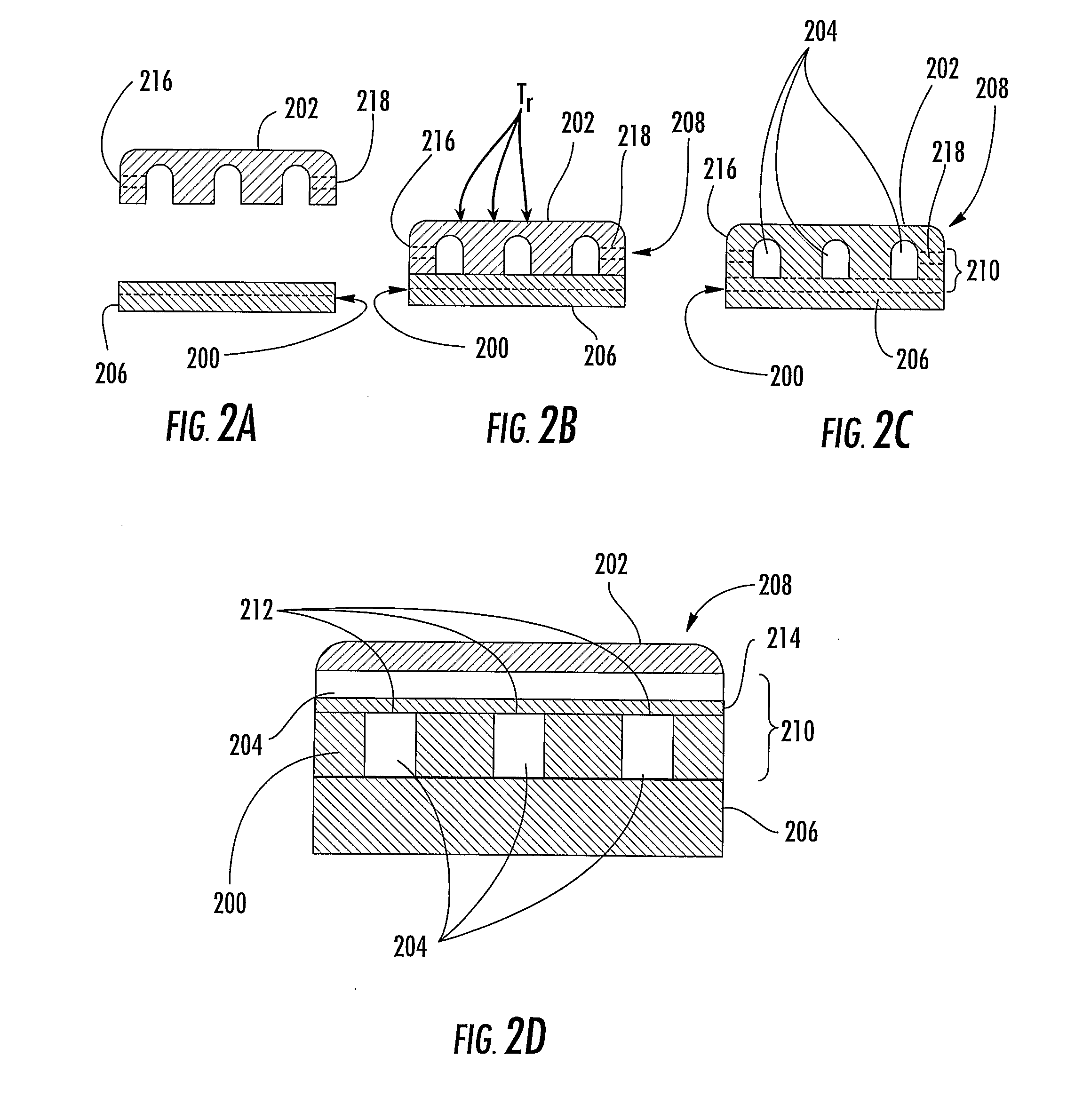
[0373] A liquid PFPE precursor encapped with methacrylate groups is blended with 1 wt % of 2,2-Azobisisobutyronitrile and poured over a microfluidics master containing 100-μm features in the shape of channels. A PDMS mold is used to contain the liquid in the desired area to a thickness of about 3 mm. The wafer is then placed in an oven at 65° C. for 2-3 hours under nitrogen purge. Separately, a second master containing 100-μm features in the shape of channels is spin coated with a small drop of the liquid PFPE precursor over top of it at 3700 rpm for 1 minute to a thickness of about 20 μm. The wafer is then placed in an oven at 65° C. for 2-3 hours under nitrogen purge. Thirdly, a smooth, flat PFPE layer is generated by drawing a doctor's blade across a small drop of the liquid PFPE precursor across a glass slide. The wafer is then placed in an oven at 65° C. for 2-3 hours under nitrogen purge. The thicker layer is then remov...


PUM

PropertyMeasurementUnit
Young's modulusaaaaaaaaaa
surface energyaaaaaaaaaa

Abstract

The presently disclosed subject matter provides functional perfluoropolyether (PFPE) materials for use in fabricating and utilizing microscale devices, such as a microfluidic device. The functional PFPE materials can be used to adhere layers of PFPE materials to one another or to other substrates to form a microscale device. Further, the presently disclosed subject matter provides a method for functionalizing the interior surface of a microfluidic channel and/or a microtiter well. Also the presently disclosed subject matter provides a method for fabricating a microscale structure through the use of a sacrificial layer of a degradable material.

Description

CROSS REFERENCE TO RELATED APPLICATIONS [0001] This application is based on and claims priority to U.S. Provisional Patent Application Ser. No. 60 / 544,905, filed Feb. 13, 2004, which is incorporated herein by reference in its entirety.GOVERNMENT INTEREST [0002] This invention was made with U.S. Government support from Office of Naval Research No. N000140210185 and STC program of the National Science Foundation under Agreement No. CHE-9876674. The U.S. Government has certain rights in the invention.TECHNICAL FIELD [0003] The presently disclosed subject matter relates to functional materials and their use for fabricating and utilizing micro- and nano-scale devices. ABBREVIATIONS [0004] AC=alternating current [0005] Ar=Argon [0006]° C.=degrees Celsius [0007] cm=centimeter [0008] 8-CNVE=perfluoro(8-cyano-5-methyl-3,6-dioxa-1-octene) [0009] CSM=cure site monomer [0010] CTFE=chlorotrifluoroethylene [0011] g=grams [0012] h=hours [0013] 1-HPFP=1,2,3,3,3-pentafluoropropene [0014] 2-HPFP=1,1,...

Claims


Application Information

Patent Timeline
Patent Type & Authority Applications(United States)
IPC IPC(8): B32B7/02B05D1/40B05D3/02C08F16/24C12M1/40H05H1/00G01F13/00C08G73/24B67D5/00B05D3/06B01L99/00B67D99/00
CPCB01L3/0268Y10T428/24B01L3/502738B01L7/52B01L2200/12B01L2300/0816B01L2400/0481B01L2400/0655B81B2201/051B81C1/00206B81C99/0085B81C2201/019B81C2201/034F16K99/0001F16K99/0015F16K99/0034F16K2099/008F16K2099/0084B29C66/9121Y10T428/13B01L3/502707Y10T137/0329
Inventor DESIMONE, JOSEPH M.ROLLAND, JASON P.ROTHROCK, GINGER DENISON
Owner THE UNIV OF NORTH CAROLINA AT CHAPEL HILL
Why Eureka
Try Eureka