Prepreg for Printed Wiring Board, Metal Foil Clad Laminate and Printed Wiring Board, and, Method for Manufacturing Multi-Layer Printed Wiring Board
Active Publication Date: 2007-12-06
HITACHI CHEM CO LTD
View PDF17 Cites 9 Cited by
Summary
Abstract
Description
Claims
Application Information
AI Technical Summary
This helps you quickly interpret patents by identifying the three key elements:
Problems solved by technology
Method used
Benefits of technology
Benefits of technology
[0014] It is therefore an object of the present invention, which was conceived to resolve the problems inherent in the prior art, to provide a printed wiring board prepreg and metal foil-clad laminate having a small water absorption rate and dimensional variation rate, and superior bending properties when a printed wiring board is formed, together with a method of manufacturing a multilayer printed wiring board using these.
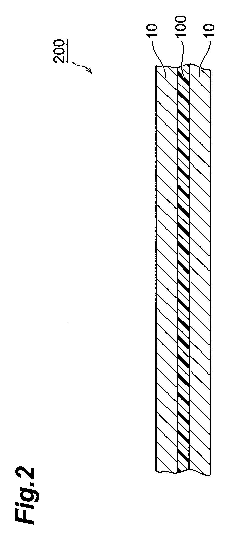
[0034] The printed wiring board prepreg and metal foil-clad laminate of the present invention have a low water absorption rate and dimensional variation rate, and can be bent by 90°, and by using these as a printed wiring board, superior bending properties can be obtained.
[0036] The present invention provides a printed wiring board prepreg, a metal foil-clad laminate and a printed wiring board, and a method of manufacturing a multilayer printed wiring board wherein, when a multilayer printed wiring board comprising a projecting inner layer board such as a rigid-flexible substrate is formed, resin exudation from the prepreg to the inner layer board is small, bending properties are good, and there is no scatter of resin powder from the prepreg.
Problems solved by technology
The rigid-flexible substrate requires a complex multilayer bonding process (see Patent Document 1), and the commercial production tact time is very long.
In the case of a resin film, it is common to use resin compositions which are different also from the aforesaid rigid laminate or flexible resin film, and if they are to be used as a multilayer printed wiring board, it gives rise to great limitations in circuit processing and press conditions during multilayer bonding.
As materials of various resin types are involved, circuit processing is more complicated than that with a single resin type.
This complexity increases commercial production tact time, and directly results in price increase.
There is also the problem that a film of these resins alone has a high water absorption compared with a metal foil-clad laminate containing a prior art glass fabric or nonwoven glass fabric, and dimensional stability during etching of the metal foil or after circuit processing is low.
For this reason, sufficient improvements in processing and connection of imperceptible wiring cannot be expected.
However, in all of these techniques, the resin layer is used alone, so there is a limit to reduction of moisture absorption or thermal expansion coefficient, and the potential loss in the reliability of connections in increasingly high density printed wiring boards is a matter of concern.
For printed wiring boards, these problems cause broken circuit wiring or short circuits, and are fatal defects.
However, although these methods are effective in the manufacture of ordinary multilayer printed wiring boards, they tend to cause plastic defects when a prepreg cut smaller than an inner layer board is disposed on the inner layer board, and a rigid-flexible substrate is used up to the ends of the heated prepreg.
The procedure is also very complex, and there is a possibility of causing various defects such as substrate warp and chipping.
Method used
Image
Click on the blue label to locate the original text in one second.
Reading with bidirectional positioning of images and text.
Examples
blending example 1
[0087] The resin material shown below was diluted with methyl ethyl ketone to 30 wt % resin solids, and a thermosetting resin composition varnish was thus produced.
[0092] The resin material shown below was diluted with methyl ethyl ketone to 30 wt % resin solids, and a thermosetting resin composition varnish was thus produced.
[0097] The resin material shown below was diluted with methyl ethyl ketone to 30 wt % resin solids, and a thermosetting resin composition varnish was thus produced.
PUM
Property
Measurement
Unit
Temperature
aaaaa
aaaaa
Length
aaaaa
aaaaa
Thickness
aaaaa
aaaaa
Abstract
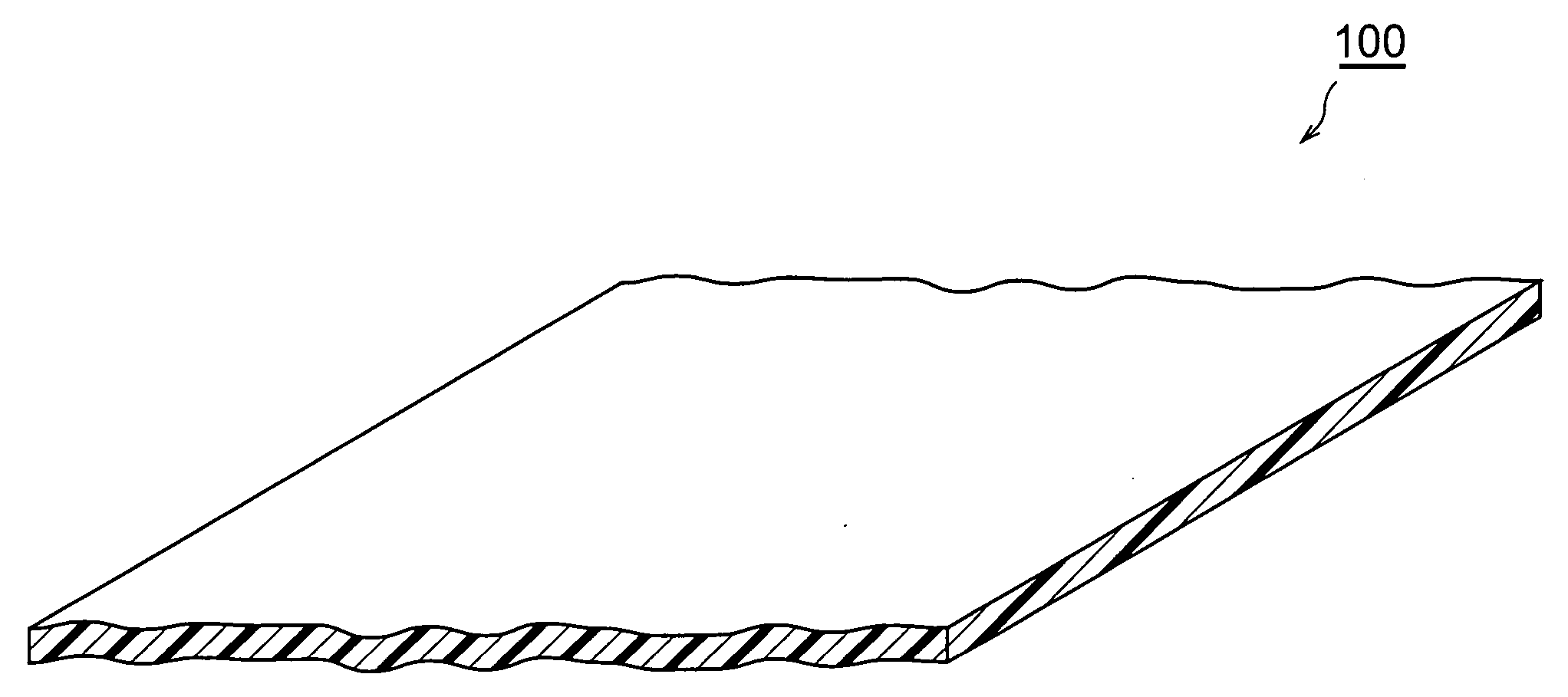
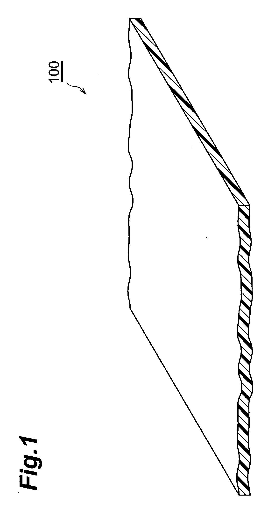
A printed wiring board prepreg according to the present invention is a printed wiring board prepreg obtained by impregnation-drying of a base material with a thermosetting resin composition, and when it is bent by 90°, cracks do not occur in the base material.
Description
TECHNICAL FIELD [0001] This invention relates to a prepreg used for a printed wiring board, a metal foil-clad laminate and a printed wiring board, and a method of manufacturing a multilayer printed wiring board. BACKGROUND ART [0002] With the rapid growth of information terminal electronic devices, electronic devices are becoming more compact and thinner. Moreover, as the functions of electronic devices such as mobile phones continue to increase, there is a demand to interconnect various high performance modules including cameras and high-density printed wiring boards. [0003] The number of mounted electronic parts is also increasing rapidly, and since a large number of electronic parts have to be mounted in the limited space of a printed wiring board, not only the rigid printed wiring boards of the prior art, but freely bendable soft substrates are required. As a bendable printed wiring board material, a polyimide-based thermoplastic resin film is mainly used. However, since thermop...
Claims
Application Information
Patent Timeline
Application Date:The date an application was filed.
Publication Date:The date a patent or application was officially published.
First Publication Date:The earliest publication date of a patent with the same application number.
Issue Date:Publication date of the patent grant document.
PCT Entry Date:The Entry date of PCT National Phase.
Estimated Expiry Date:The statutory expiry date of a patent right according to the Patent Law, and it is the longest term of protection that the patent right can achieve without the termination of the patent right due to other reasons(Term extension factor has been taken into account ).
Invalid Date:Actual expiry date is based on effective date or publication date of legal transaction data of invalid patent.

