Electronic device and method of manufacturing and electronic device

Inactive Publication Date: 2007-12-06
NEC LIGHTING
View PDF6 Cites 6 Cited by
  • Summary
  • Abstract
  • Description
  • Claims
  • Application Information

AI Technical Summary

Benefits of technology

[0020]An object of the present invention is to provide an electronic device cap

Problems solved by technology

Therefore, even if the area of metal layer 101 is widened in order to improve the heat releasing property, sufficient heat releasing effect will not be not attainable.
However, solder wettability of the graphite sheet, in which carbon is used as the main material, is low and it was difficult to provide a solder layer to implement sub-mount on the graphite sheet.
Therefore, although a high heat transfer coefficient can apparently be obtained by bringing the graphite sheet and the sub-mount into junction, it was impossible to realize junction between the graphite sheet and the sub-mount with the solder layer.
However, the thermal conductivity of grease is smaller than the thermal conductivity of solder.
Therefore, it is impossible to take full advantage of the heat diffusion property of the graphite sheet as well.
Also, Japanese Patent Laid-Open

Method used


Image

  • Electronic device and method of manufacturing and electronic device
  • Electronic device and method of manufacturing and electronic device
  • Electronic device and method of manufacturing and electronic device

Examples


first embodiment

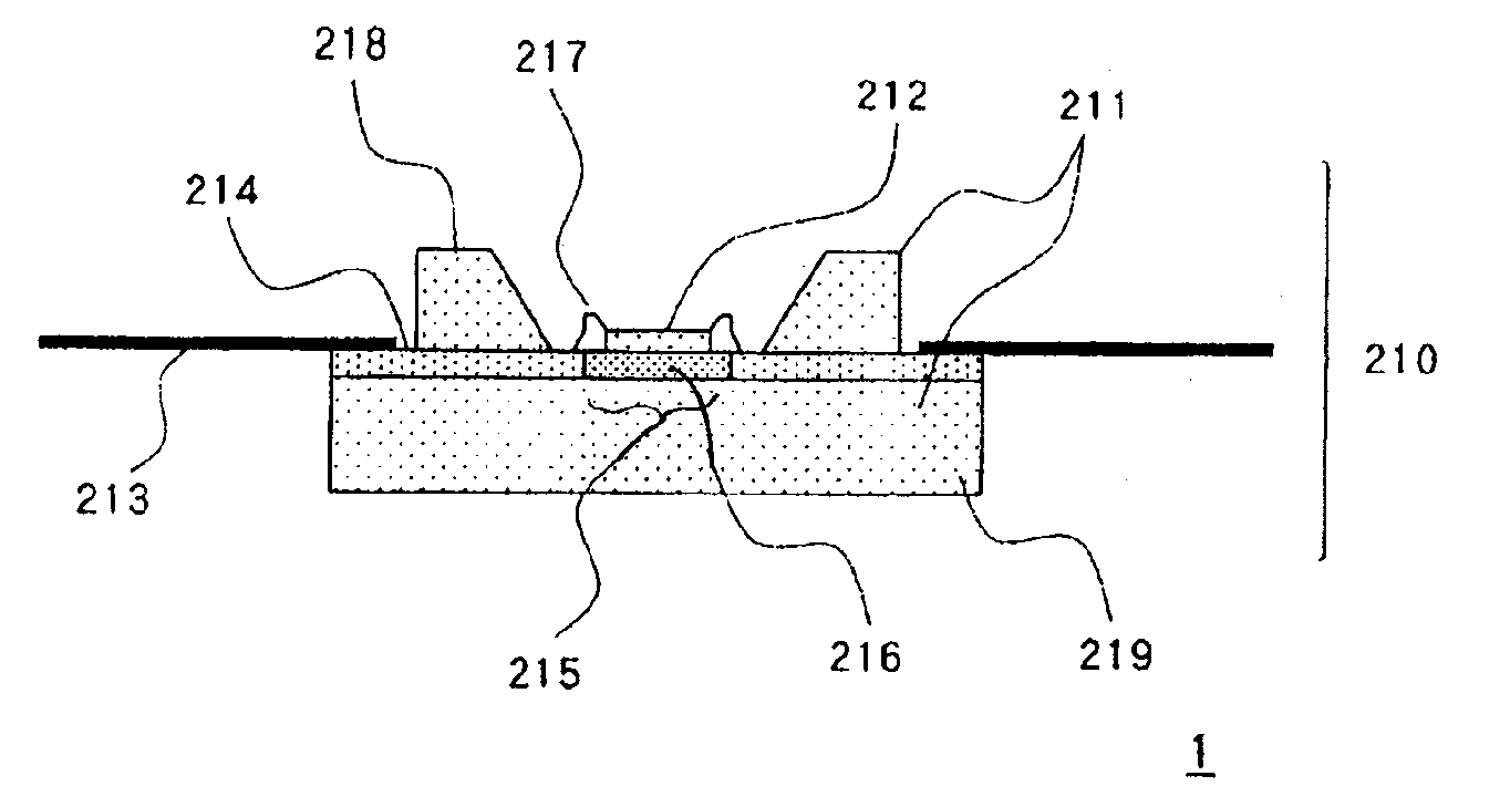
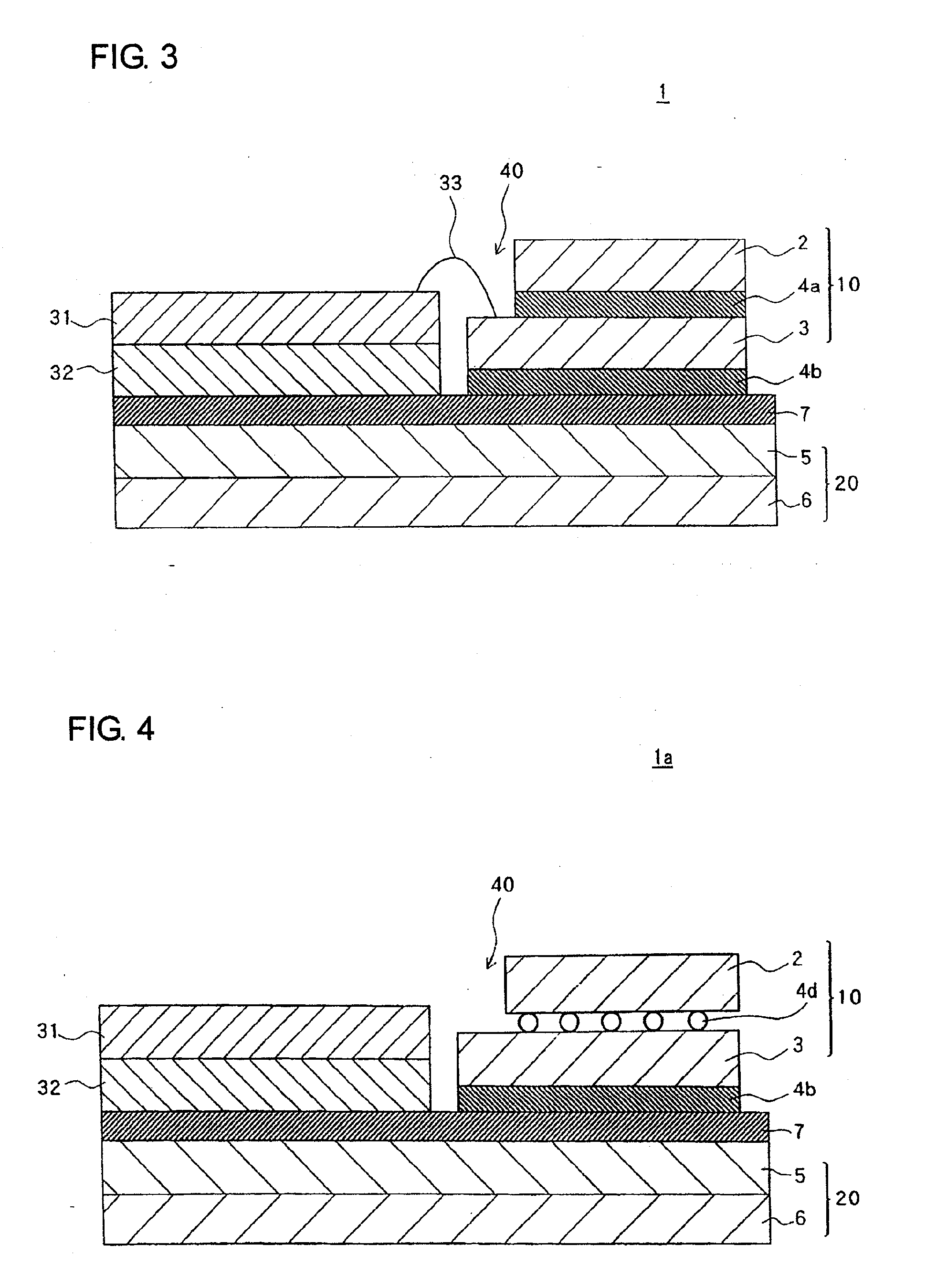
[0070]FIG. 3 illustrates a schematic section illustrating a configuration of electronic device 1 of the present embodiment.

[0071]Electronic device 1 has heating structure 10 configured by mounting LED chip 2 on sub-mount 3 on heat releasing structure 20 comprising first metal layer 6 and graphite layer 5. Second metal layer 7 is provided on graphite layer 5. Heating structure 10 and heat releasing structure 20 are brought into junction with second solder layer 4b. That is, sub-mount 3 of heating structure 10 and second metal layer 7 of heat releasing structure 20 are brought into junction with second solder layer 4b.

[0072]Heat releasing structure 20 is for diffusing heat from LED chip 2 to the exterior atmosphere and includes first metal layer 6 made of metal with good heat conductivity and graphite layer 5 with good heat conductivity in the plane direction. Graphite layer 5 is provided by being stacked on the plane on the side of first metal layer 6 where LED chip 2 is mounted.

[00...

second embodiment

[0106]A schematic section illustrating configuration of electronic device 51 of the present embodiment is illustrated in FIG. 6.

[0107]As LED chip 52 of electronic device 51 of the present embodiment is configured by P pole 52a and N pole 52b provided on the upper plane and is mounted directly on second metal layer 7 without intervention of a sub-mount. Since the other basal configuration is the same as in the first embodiment described above, detailed description will be omitted.

[0108]On the lower plane of LED chip 52 where P pole 52a and N pole 52b are not provided, a plating layer (for example, gold plating) is formed so that there will be good solder wettability. LED chip 52 causes plane to face second metal layer 7 and is brought into junction by means of solder layer 4c. P pole 52a is electrically connected to first wiring layer 31a by first wiring wire 33a. In addition, N pole 52b is electrically connected to second wiring layer 31b by second wiring wire 33b.

[0109]The first e...

third embodiment

[0118]For the present embodiment, an electronic device comprises a graphite layer and a second metal layer to realize high heat conductivity. A method for manufacturing the electronic device comprising, in particular, a connector will be described. Here, in the following description, electronic device 1 illustrated in the first embodiment will be used as an example.

[0119]In a case in which the idea is to establish an electrical connection between another apparatus and electronic device 1, using an electric-wire to link wiring layer 31 of electric device 1 to the other apparatus can be considered. In that case, the electric wire will be soldered to wiring layer 31. However, as described above, electronic device 1 is highly heat conductive. Therefore, the heat of the soldering iron will be absorbed by electronic device 1 and there will be a failure in producing an adequate alloy layer, resulting in mechanically incomplete soldering. That is, a method of carrying out soldering onto wir...


PUM


Abstract

An electronic device includes a heating structure including a sub-mount for mounting an LED chip thereon, a first solder layer for bringing the LED chip and the sub-mount into junction and a heat releasing structure including a first metal layer and a graphite layer stacked onto the first metal layer, wherein the heating structure is mounted on the graphite layer side of the heat releasing structure. The electronic device includes a second metal layer being present on a plane in the graphite layer opposite to a plane where the first metal layer is stacked; and the second metal layer and the sub-mount are brought into junction with a second solder layer so that the heating structure and the heat releasing structure are thereby brought into junction.

Description

BACKGROUND OF THE INVENTION[0001]1. Field of the Invention[0002]The present invention relates to electronic devices which diffuse and radiate heat from heating elements with graphite and a method of manufacturing electronic devices.[0003]2. Description of the Related Art[0004]Efficient radiation of heat generated by pyrogenic parts is extremely important for preventing parts from malfunctioning and for ensuring longevity of products. Therefore, conventionally, various kinds of heat releasing material are used in electric and electronic devices having parts accompanying heat generation. In particular, in recent years, as progress is made in reducing the size and improving the sophistication and performance of electronic devices, graphite sheets made of graphite as main material are used in order to efficiently release heat generated from large-scale integrated CPU or LED. A graphite sheet is thermally anisotropic and has a good heat conductive property in the of plane direction. Ther...

Claims


Application Information

Patent Timeline
IPC IPC(8): H05B3/06H01L33/64H01L33/62
CPCH05B3/145H05B3/30H01L2224/48091H01L2924/00014
Inventor OKIMURA, KATSUYUKI
Owner NEC LIGHTING
Why Eureka
Try Eureka