

Optoelectronic devices utilizing materials having enhanced electronic transitions
- Summary
- Abstract
- Description
- Claims
- Application Information
AI Technical Summary
Problems solved by technology
Method used
Image

Examples
example 1
Mid-IR Detector or Emitter Using Bismuth
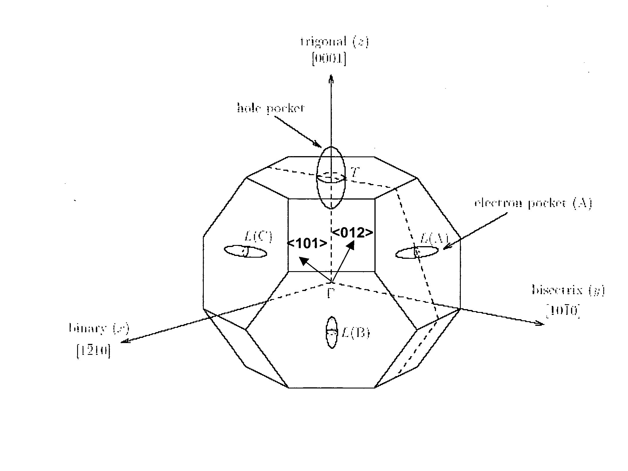
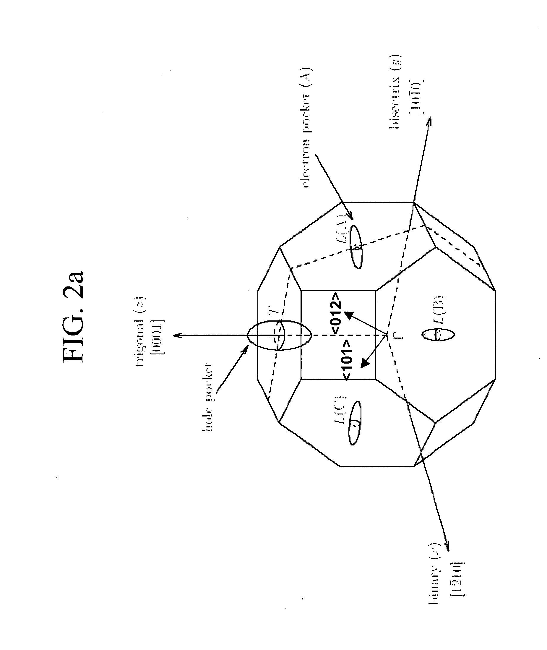
[0047] Bismuth is a narrow band gap semi-metal with a very unusual band structure, which is shown in FIG. 2b. The T point valence band crosses the Fermi energy (EF) so the band edge is above the Fermi energy leaving lots of empty electron states (holes). The L point valence band edge is below the Fermi energy and is therefore mostly filled with electrons. Because both of these states are curved in the same direction (as opposed to a valence and conduction band pairs), the joint density of states is large. Furthermore, because there is a hole pocket at the T point and an electron pocket at the L point, many electrons can be excited from the L point valence band to the T point valence band. In bulk bismuth, however, this transition, which is predicted to be around 0.13 eV at room temperature, is indirect and weak.
[0048] In bismuth nano-wires, the symmetry arguments break down and the L to T point transition becomes allowed. Hence, bismuth nano...
example 2
Red Emitter Using Silicon Nano-Wires that Utilize the Effect of Interface Mixing
[0052] Numerous studies have looked into the photoluminescence in silicon quantum structures. These structures include amorphous silicon, which has been shown to contain quantum dots.
[0053] Several theories have been proposed to explain the photoluminescence between 550 nm and 700 nm observed for silicon, but none of the theories explain all the data. It is very likely that interface mixing enhances the coupling between the gamma (Γ) and L point and this transition is causing the observed photoluminescence. If this is indeed the cause, the ideal structure for maximizing this luminescence will comprise high purity silicon having interfaces in the direction and only slight doping levels, as too high doping will decrease the diameter required to observe the photoluminescence.
example 3
Intermediate Band Solar Cell Using Silicon Nano-Wires Utilizing Interface Mixing
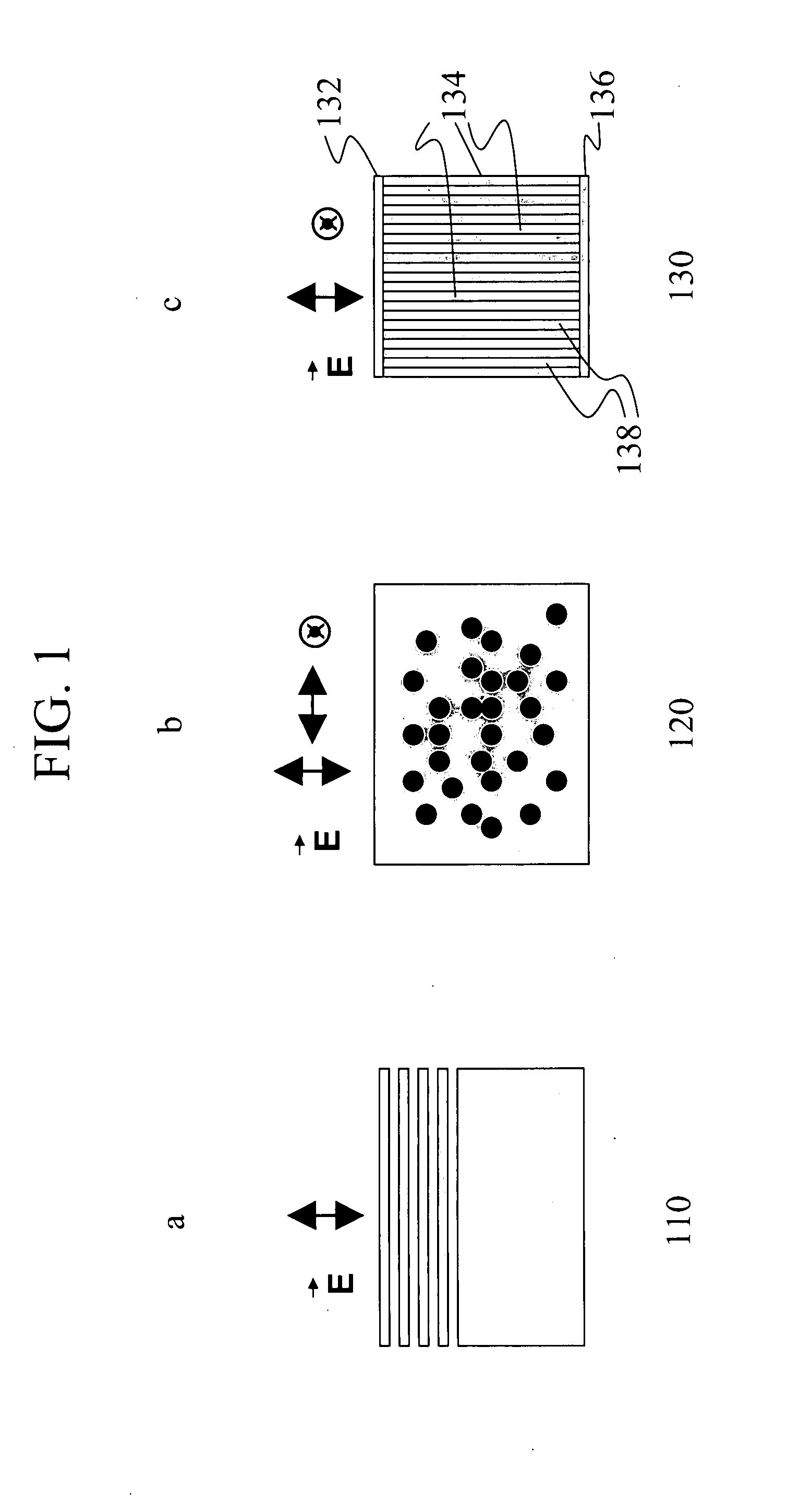
[0054] One approach to fabricating intermediate band solar cells that has been proposed is sandwiching quantum dots between two semiconductors. Obtaining electrical contact to the quantum dots, however, is difficult. By utilizing interface mixing, a single material can be used to provide both levels in the intermediate band solar cell. The strength of coupling between the ground state and the two excited states can be optimized for solar cell efficiency by changing the orientation and diameter of nano-wires 134. Coincidentally, silicon has two band gaps that together are very near the optimal energies for an intermediate band solar cell. The smallest band gap is at 1.12 eV at the delta point in the X direction. Another carrier pocket exists at the L point and is predicted to be between 1.6 eV and 2.1 eV. Intermediate band gap solar cells with band gaps at 1.12 eV and 1.9 eV and having efficiencies of ov...
PUM
| Property | Measurement | Unit |
|---|---|---|
| Diameter | aaaaa | aaaaa |
| Diameter | aaaaa | aaaaa |
| Temperature | aaaaa | aaaaa |
Abstract
Description
Claims
Application Information