Non-Volatile Memory Embedded In A Conventional Logic Process And Methods For Operating Same

a logic process and non-volatile memory technology, applied in the field of non-volatile memory, can solve the problems of incompatibility with a conventional logic process, charge trapping layer is not generally available in an asic or logic process, and is incorporated in the transistor used for logic gates, etc., to achieve low cost, minimize the probability of over-erasure of memory cells, and high efficiency

Inactive Publication Date: 2007-12-06
MOSYS INC
View PDF49 Cites 56 Cited by
  • Summary
  • Abstract
  • Description
  • Claims
  • Application Information

AI Technical Summary

Benefits of technology

[0015]The non-volatile memory cell array can be laid out in different configurations and be biased in different manners in the various embodiments. In one embodiment, each non-volatile memory cell of the array includes a PMOS access transistor and an NMOS capacitor structure, which share a common floating gate. The PMOS access transistors associated with each row of the array are fabricated in a corresponding isolated n-well region. Each isolated n-well region is biased by a separate control voltage. The drains of the PMOS access transistors associated with each column of the array are connected by a corresponding bit line. The floating gates of the non-volatile memory cells in each row of the array are coupled to a corresponding word line. This configuration allows the memory cells to be programmed in a random per bit manner using a band-to-band tunneling mechanism to inject electrons into the desired floating gates. During programming, the current through each of the programmed memory cells is monitored individually so as to avoid the over-program problem. This configuration also allows the memory cells to be erased using a Fowler-Nordheim tunneling mechanism to simultaneously remove electrons from the floating gates of all memory cells in a sector. Using Fowler-Nordheim tunneling to remove electrons from the floating gates has the advantage that the process is self-limiting. This self-limitation minimizes the probability of over-erasing the memory cells.
[0016]The non-volatile memory of the present invention can be included in a system-on-a-chip (SoC) architecture, along with dynamic memory configured to implement one-transistor static random access memory (1T-SRAM) with hidden refresh and other logic functions. The SoC can be fabricated using a conventional logic process to realize a highly optimized SoC produced at a low cost.

Problems solved by technology

However, traditional processes for fabricating non-volatile memory, which typically use stacked gate or split-gate memory cells, are not compatible with a conventional logic process.
However, this charge trapping layer is not generally available in an ASIC or logic process, nor is it incorporated in transistors used for logic gates.
Over-erase or over-programming causes the threshold voltage of the cell transistor to have a value outside the targeted operating range and may result in functional failure of the memory device.
More importantly, due to process variation and defects, some of the memory cells in a memory array can be programmed or erased much faster or slower than the other memory cells.
However, in Flash memory, where a block of memory cells are erased simultaneously, monitoring individual cell currents during erase may be too time consuming to be practical.
Over-erased cells in a flash memory array may cause read failures in the array.
If too many electrons are injected into the floating gate of a PMOS access transistor of a non-volatile memory cell during an erase operation (as a result of the difficult to control band-to-band tunneling mechanism), the threshold voltage of the PMOS access transistor will increase to an undesirable level (i.e., the PMOS access transistor will become undesirably conductive).
The over-erase condition may eventually get to the point where programming is no longer possible (within practical limits).
Thus, read operations to an over-erased non-volatile memory cell (as well as read operations to adjacent non-volatile cells in the same array) will produce erratic and invalid results.
The over-erase condition will eventually lead to device failure.

Method used


Image

  • Non-Volatile Memory Embedded In A Conventional Logic Process And Methods For Operating Same
  • Non-Volatile Memory Embedded In A Conventional Logic Process And Methods For Operating Same
  • Non-Volatile Memory Embedded In A Conventional Logic Process And Methods For Operating Same

Examples


Embodiment Construction

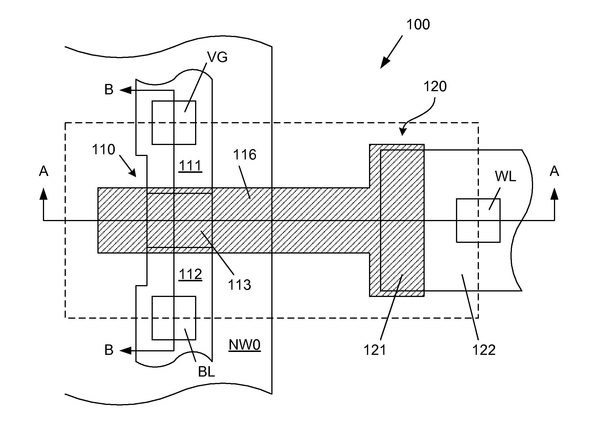
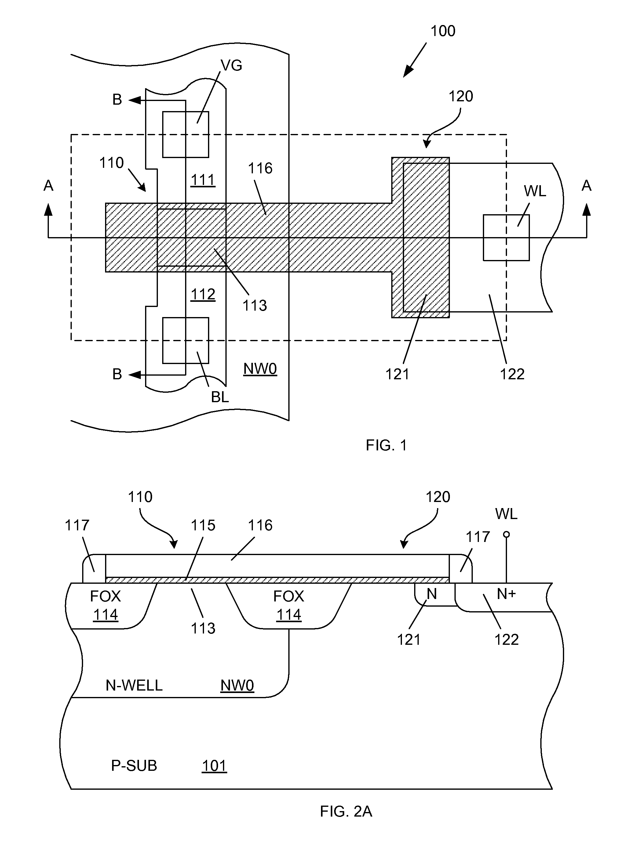
[0030]FIG. 1 is a top layout view of a non-volatile memory cell 100 that can be fabricated using a conventional logic process. FIG. 2A is a cross-sectional view of non-volatile memory cell 100 along section line A-A. FIG. 2B is a cross-sectional view of non-volatile memory cell 100 along section line B-B. The structure and fabrication of non-volatile memory cell 100 is largely described in commonly-owned U.S. Pat. No. 6,512,691 to Hsu et al., which is hereby incorporated by reference in its entirety.

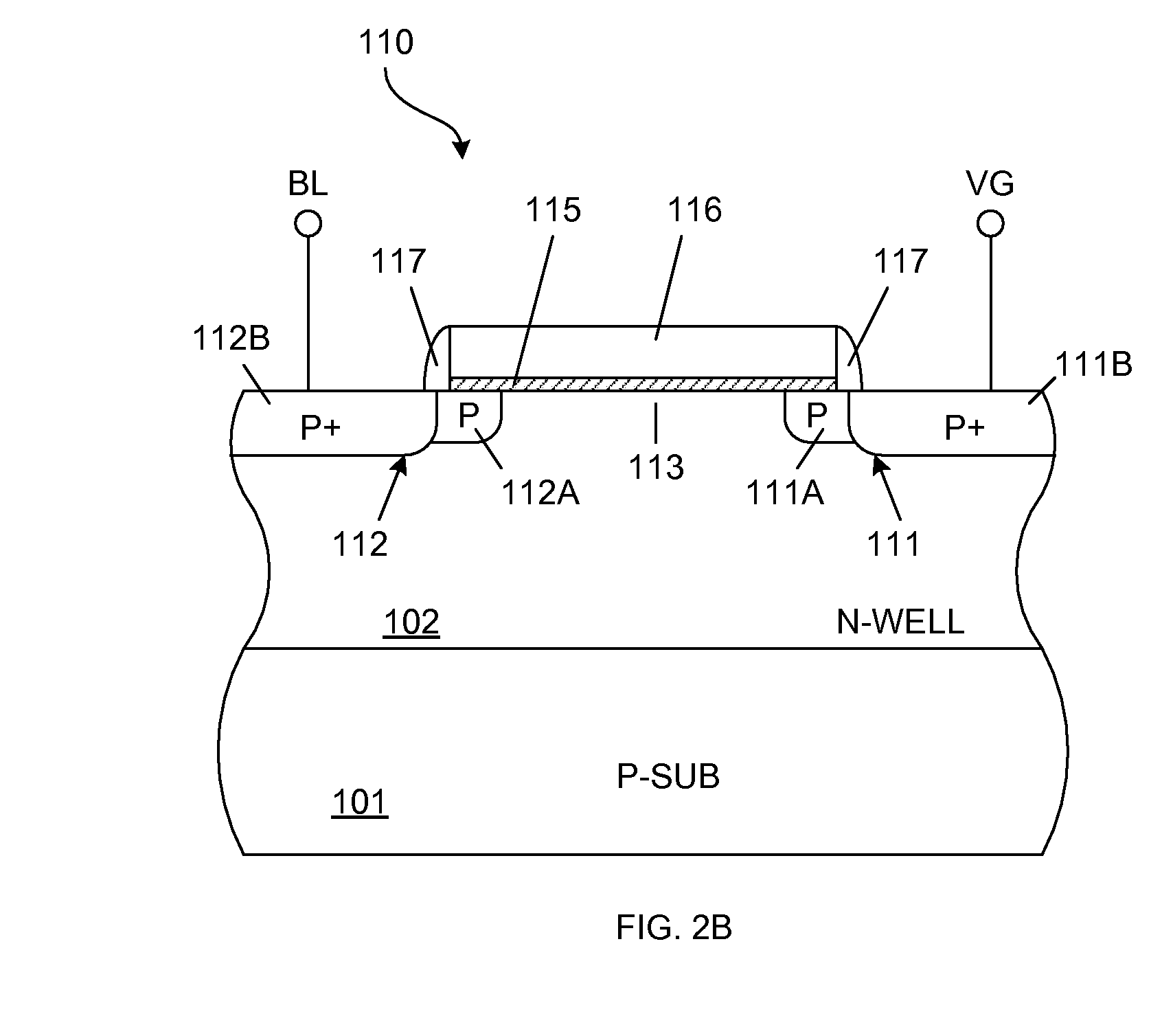
[0031]Non-volatile memory cell 100 is fabricated in a p-type monocrystalline semiconductor substrate 101 (e.g., silicon). Non-volatile memory cell 100 includes a PMOS access transistor 110, having a p-type source 111 and a p-type drain 112 fabricated in an n-well region NW0. Source region 111 includes lightly doped source 111A and p+ source contact region 111B. Drain region 112 includes lightly doped drain 112A and p+ drain contact region 112B. A channel region 113 is located between sou...


PUM


Abstract

A non-volatile memory system including an array of cells, each having an access transistor and a capacitor sharing a floating gate. The access transistors in each row are fabricated in separate well regions, which are independently biased. Within each row, the source of each access transistor is coupled to a corresponding virtual ground line, and each capacitor structure is coupled to a corresponding word line. Alternately, the source of each access transistor in a column is coupled to a corresponding virtual ground line. Within each column, the drain of each access transistor is coupled to a corresponding bit line. Select memory cells in each row are programmed by band-to-band tunneling. Bit line biasing prevents programming of non-selected cells of the row. Programming is prevented in non-selected rows by controlling the well region voltages of these rows. Sector erase operations are implemented by Fowler-Nordheim tunneling.

Description

RELATED APPLICATIONS[0001]This is a continuation in part of U.S. patent application Ser. No. 11 / 341,881-2960 “Method To Increase Charge Retention Of Non-Volatile Memory Manufactured In A Single-Gate Logic Process” by Gang-feng Fang, Wingyu Leung, and Dennis Sinitsky.FIELD OF THE INVENTION[0002]The present invention relates to non-volatile memory (NVM). More particularly, this invention relates to non-volatile memory cells fabricated using an application specific integrated circuit (ASIC) or conventional logic process. This invention further relates to a method of operating a non-volatile memory to ensure maximum data retention time. The invention also relates to a system-on-chip (SoC) architecture which includes both non-volatile memory and dynamic random access memory (DRAM) that operates like static random access memory (SRAM), wherein the SoC is fabricated using a conventional logic process.RELATED ART[0003]For system-on-chip (SoC) applications, it is desirable to integrate many ...

Claims


Application Information

Patent Timeline
Patent Type & Authority Applications(United States)
IPC IPC(8): G11C16/04G11C11/34
CPCG11C16/0416G11C16/10G11C16/3477H01L27/11558H01L27/115H01L27/11519H01L27/11521G11C2216/10H10B69/00H10B41/10H10B41/30H10B41/60H10B63/80
Inventor FANG, GANG-FENGLEUNG, WINGYU
Owner MOSYS INC
Why Eureka
Try Eureka