Organic semiconductor device and method for manufacturing the same

a technology of organic el and semiconductors, applied in the direction semiconductor devices, solid-state devices, etc., can solve the problems of large manufacturing costs, easy control of a very small amount of dopant, and relatively low manufacturing cost of organic el devices

Inactive Publication Date: 2007-12-06
PARK BYOUNG CHOO
View PDF2 Cites 38 Cited by
  • Summary
  • Abstract
  • Description
  • Claims
  • Application Information

AI Technical Summary

Benefits of technology

[0013]An object of the present invention is to provide an organic semiconductor device including the organic EL device

Problems solved by technology

However the dry process requires a high vacuum environment, the manufacturing conditions should be controlled carefully, and thus the process for fabricating EL devices is complex, resulting in the large manufacturing costs.
(2) It is easy to control a very small amount of dopant, which is difficult in the dry process.
(4) The organic EL layer of the organic EL device can be easily formed relatively and thus the manufacturing cost of the organic EL device is relatively low.
Therefore, it is difficult to balance injection and transportation of holes and electrons.
As a result, a recombination possibility is decreased and then it is difficult to get sufficient light-emitting efficiency.
However, the device having the organic EL layer produced with this method also has a low light-emitting efficiency and requires a high driving voltage.
However the maximum luminance of the EL device which was fabricated according

Method used


Image

  • Organic semiconductor device and method for manufacturing the same
  • Organic semiconductor device and method for manufacturing the same
  • Organic semiconductor device and method for manufacturing the same

Examples


example 1

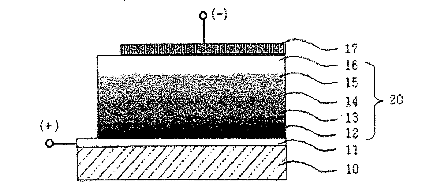
Manufacturing the Organic EL Device Having the Single-Layered Thin Film Structure of Graded Junction Type Including the Organic Salts

[0068]A glass substrate (0.7 mm) coated with Indium-Tin-Oxide(ITO) having 15 Ω was ultrasonically washed in a commercially available cleaning agent, and then washed with deionized water. The organic compound solution was prepared by dissolving the organic materials in 6.0 g of mixture solution (chloroform:dichloroethane=1:3), wherein the organic materials include 6.5 mg of PVK (poly-N-vinylcarbazole) as the charge carrier binder resin, 6.5 mg of α-NPD as the hole transporting material, 6.5 mg of Alq3 as the green light-emitting and electron injecting material, 0.2 mg of C545T as the green light-emitting dopant and 0.5 mg of Bu4N-BF4 as the organic salts. The boiling point of chloroform and dichloroethane(ClCH2CH2Cl) were 62° C. and 82° C. respectively. The organic compound solution was filtered through 0.2 μm Teflon filter. Thereafter, the organic com...

example 2

Manufacturing the Organic EL Device Having the Single-Layered Thin Film Structure of the Graded Junction Type Including the Inorganic Salts

[0072]Except for using LiF inorganic salt instead of Bu4N-BF4 organic salt, the organic EL device was manufactured in the same manner as described in Example 1. As shown in Table 1, the EL light-emitting initiation voltage(Von-set) of the EL device was about 5V, the current flowing through the EL device and the light-emitting luminance at the voltage of 10V were 7.4 mA and about 114 cd / m2 respectively. The EL device emitted the stable and uniform green light (520 nm) at the voltage of 10V for a long time. Thus, the EL device had the 3 times increased light-emitting luminance at 10V in comparison with the standard EL device of Comparative Example 1.

example 3

Manufacturing the Organic EL Device of the Uniformly Distributed Single-Layered Thin Film Structure Including the Organic Salts

[0073]Except for using chloroform instead of the mixture solution of chloroform and dichloroethane, the EL device was manufactured in the same manner as described in Example 1. As shown in Table 1, the EL light-emitting on-set voltage(Von-set) of the EL device was about 5V, the current flowing through the EL device and the light-emitting luminance at the voltage of 10V were 2.5 mA and about 260 cd / m2 respectively. The EL device emitted the stable and uniform green light at the voltage of 10V for a long time. Thus, the EL device had the 6.8 times increased light-emitting luminance at 10V in comparison with the standard EL device of Comparative Example 1.


PUM

PropertyMeasurementUnit
Temperatureaaaaaaaaaa
Percent by massaaaaaaaaaa
Electric potential / voltageaaaaaaaaaa

Abstract

An organic semiconductor device having enhanced uniformity of light-emission and excellent luminance with relatively low driving voltage and manufactured by a wet process and method for manufacturing the same are disclosed. The method for manufacturing an organic semiconductor device, comprises the steps of: forming a first electrode on a substrate; forming an organic semiconductor layer including an ionic salt by coating an organic compound solution on the first electrode and removing an organic solvent from the coated organic compound solution, wherein the organic compound solution includes the organic solvent, the ionic salt and organic semiconductor compounds; forming a second electrode having the opposite electric potential to the first electrode on the organic semiconductor layer including the ionic salt; and treating the organic semiconductor layer including the ionic salt with thermal annealing and electrical annealing simultaneously. The semiconductor device according to the present invention comprises an anode, a cathode and a semiconductor layer containing the ionic salt, preferably organic semiconductor layer formed between the anode and the cathode, wherein the anion of the ionic salt at the interface of the anode and the semiconductor layer and the cation of the ionic salt at the interface of the cathode and the semiconductor layer are uniformly distributed over whole the light-emitting surface of the EL device.

Description

FIELD OF THE INVENTION[0001]The present invention relates to an organic semiconductor device and a method for manufacturing the same, and more particularly to, an organic semiconductor device having enhanced uniformity of light-emission and excellent luminance with relatively low driving voltage and method for manufacturing the same.BACKGROUNDS OF THE INVENTION[0002]Generally, organic semiconductor devices including organic diode devices and organic transistor devices are based on the electrical semi-conductivity that relates to the HOMO(highest occupied molecular orbital) energy level and the LUMO(lowest unoccupied molecular orbital) energy level of organic materials. Examples of the organic diode devices include organic light emitting diodes and organic EL(Electroluminescent) diodes, and examples of the organic transistor devices include organic FET(Field Effect Transistors), organic TFT(Thin Film Transistors), organic SIT(Static Induction Transistors), organic top gate SIT, organ...

Claims


Application Information

Patent Timeline
IPC IPC(8): H01L51/40
CPCH01L51/0002H01L51/0026H01L51/0037H01L51/0038H01L51/0042H01L51/0059H01L2251/5346H01L51/0078H01L51/5032H01L51/5048H01L51/5088H01L51/56H01L51/0071H10K71/10H10K71/40H10K85/146H10K85/1135H10K85/114H10K85/631H10K85/657H10K85/311H10K50/135H10K50/14H10K50/17H10K71/00H10K2101/80
Inventor PARK, BYOUNG-CHOO
Owner PARK BYOUNG CHOO
Why Eureka
Try Eureka