Organic light emitting device

a light-emitting device and organic technology, applied in the direction of discharge tube/lamp details, discharge tube luminescent screens, discharge tubes/lamp details, etc., can solve the problems of difficult hole injection, difficult hole injection, and large energy barrier, so as to optimize the charge balance and improve the efficiency of the present invention. the effect of life tim

Inactive Publication Date: 2007-12-13
SAMSUNG MOBILE DISPLAY CO LTD
View PDF10 Cites 28 Cited by
  • Summary
  • Abstract
  • Description
  • Claims
  • Application Information

AI Technical Summary

Benefits of technology

[0039]Accordingly, the efficiency and the life time of the OLED of the present invention are improved by controlling the energy relationship between the organic layers and facilitating hole injection and optimizing charge balance.

Problems solved by technology

However, the PEDOT / PSS composition has a work function from 5.0 to 5.2 eV, and thus is not advantageous for hole injection because the energy barrier between a polyfluorene derivative having generally a highest occupied molecular orbital (HOMO) value of greater than 5.5 eV and the PEDOT / PSS composition is greater than 0.3 eV, which makes hole injection difficult.
Conventionally, it is well-known in the art that when a HIL formed on the ITO has a greater work function, ionization energy, or absolute value of HOMO than a HOMO value of the HTL and the emitting layer, the work function is 4.7 to 4.9 eV, and thus a great energy barrier is present between the ITO and the HIL, and thus hole injection becomes difficult.

Method used


Image

  • Organic light emitting device
  • Organic light emitting device
  • Organic light emitting device

Examples


manufacturing example 1

Polyaniline (PANI) Conducting Polymer Composition

[0144]Polystyrenesulfonic acid-graft-polyanyline (PSSA-g-PANI) was polymerized as a self-doping conducting material using a known synthesizing method by [W. J. Bae et al. Chem. Comm., pp 2768-2769, 2003]. In the present embodiment, the weight ratio of the PSSA polymer chain and the grafted PANI chain was 1:0.15. The number-average molecular weight of PSSA-g-PANI was 35,000. The material was melted in water to 1.0 wt %. Then, a perfluorinated ionomer (PFI) that was dispersed to 5 wt % in a solvent with a volume ratio of water to alcohol of 0.45:0.55 was purchased from Aldrich Co. and isopropyl alcohol and 5 wt % PFI were mixed in a 1.0 wt % PSSA-g-PANI solution and used as a material for forming a HIL 11. This sample was called Sample A.

manufacturing example 2

Manufacturing of PEDOT-PSS / PFI Conducting Polymer Composition

[0145]PEDOT-PSS (Model: Baytron P VP AI4083) which is refined to control the content of Na and sulfate to 5 ppm or less from H. C. Starck, which is a subsidiary of Bayer Aktien AG. Then PFI of Formula 14 was dispersed to 5 wt % in water and alcohol was purchased from Aldrich Co.

[0146](where x=1300, y=200, x=1)

[0147]Then a HIL 11 was prepared with to various compositions of each of PEDOT-PSS / PFI. The ratios of the compositions were as listed in Table 1 below.

TABLE 1Sample CodePEDOT / PSS / PFIAI40831 / 6 / 0B1 / 6 / 1.6C1 / 6 / 3.2D1 / 6 / 6.3E1 / 6 / 12.7F1 / 6 / 25.4

example 1

[0151]A 15 Ω / cm2 (150 nm) ITO glass substrate by Corning was cut to a size of 50 mm×50 mm×0.7 mm, washed using supersonic waves for 5 minutes in isopropanol alcohol and pure water, treated with ultraviolet ozone generator for 30 minutes and then used.

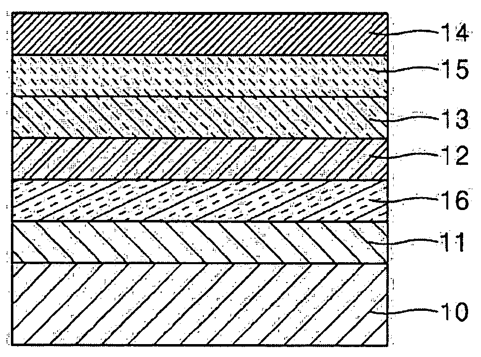
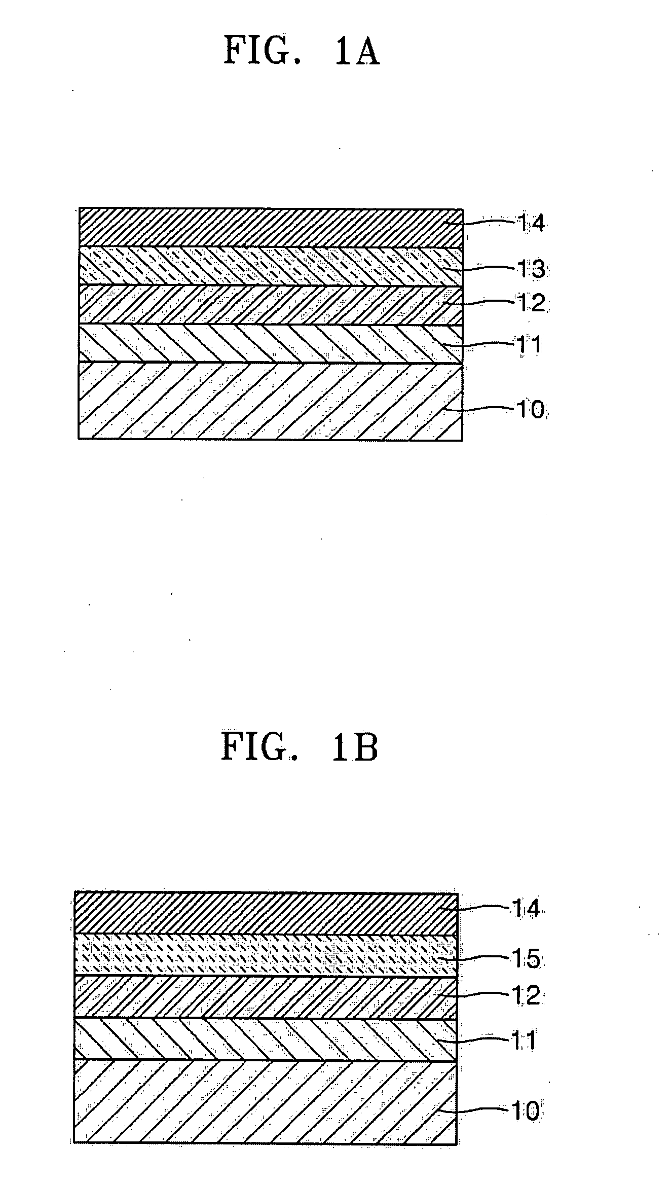
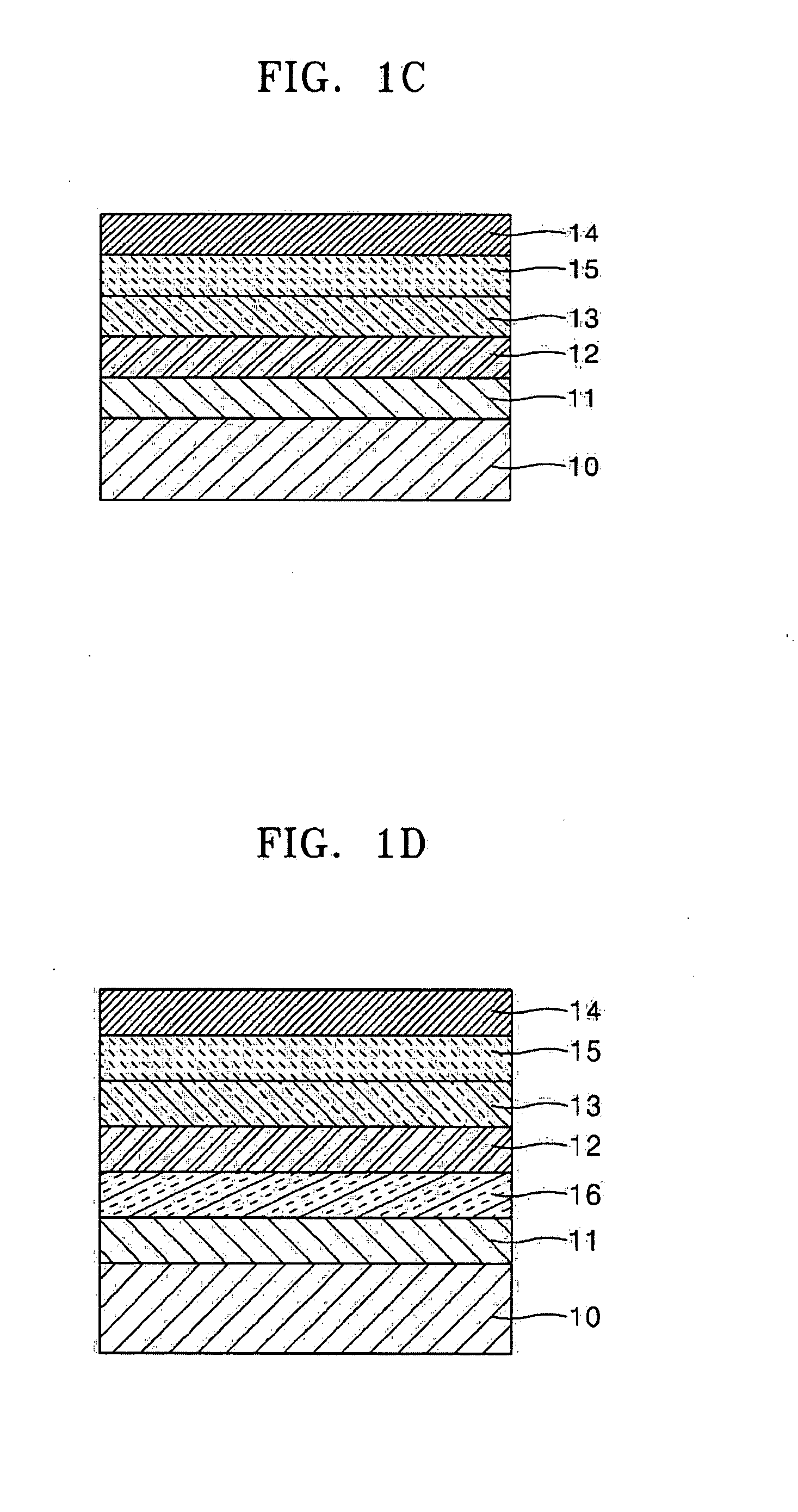
[0152]An HIL 11 was formed to a thickness of 50 nm on the ITO glass substrate by spin-coating a PEDOT-PSS / PFI conducting polymer composition solution obtained as from Manufacturing Example 2. NPB was vacuum-deposited on the HIL 11 to form an HTL 16 to a thickness of 30 nm.

[0153]An emitting layer 12 was formed to a thickness of 50 nm using ADN (9,10-di(naphti-2-il)anthracene, available from Lumtec Corp. LT-E403) as an emitting host and using DPAVBi (4,4-bis[4-(di-p-tolylamino)styryl]biphenyl, available from Lumtec Corp., LT-E605) as an emitting dopant. Then an ETL 15 was formed to a thickness of 30 nm on the emitting layer 12 by depositing Alq3 (tris(8-hydroxy-quinolinato)aluminum, available from Lumtec Corp. LT-E401) to manufacture an O...


PUM

PropertyMeasurementUnit
HOMO levelaaaaaaaaaa
LUMOaaaaaaaaaa
HOMOaaaaaaaaaa

Abstract

Provided are an organic light emitting device (OLED) comprising: a first electrode; a second electrode; a hole injection layer (HIL), a hole transporting layer (HTL), and an emitting layer sequentially formed between the first electrode and the second electrode, wherein the work function, the IP or the absolute value of the highest occupied molecular orbital (HOMO) level of the HIL is greater than or equal to the absolute value of HOMO level of the HTL. In the OLED, the energy relationships between organic layers are controlled to facilitate hole injection and optimize the charge balance. Thus the efficiency of the OLED improves and the lifetime of the OLED increases.

Description

CLAIM OR PRIORITY[0001]This application claims the benefit of Korean Patent Application No. 10-2006-0051085, filed on Jun. 7, 2006 in the Korean Intellectual Property Office, the disclosure of which is incorporated herein in its entirety by reference.BACKGROUND OF THE INVENTION[0002]1. Field of the Invention[0003]The present invention relates to an organic light emitting device (OLED), and more particularly, to an OLED in which energy relationships of layers forming the OLED are controlled to facilitate hole injection and optimize the charge balance to obtain an OLED having improved efficiency and increased lifetime.[0004]2. Description of the Related Art[0005]An organic light emitting device is a self-emissive display device using the principle that when current is applied to a fluorescent or phosphorescent organic compound thin layer (hereinafter referred to as ‘organic layer’), electrons and holes combine in the organic layer and thus light is generated. An organic light emitting...

Claims


Application Information

Patent Timeline
Patent Type & Authority Applications(United States)
IPC IPC(8): H05B33/00
CPCH01L51/0037H01L51/0059H01L51/5088H01L51/5048H01L51/0081H10K85/1135H10K85/631H10K85/324H10K50/14H10K50/17C09K11/06H05B33/22H05B33/14
Inventor LEE, TAE-WOOPARK, JONG-JINKIM, MU-HYUNCHANG, SEUNG-WOOK
Owner SAMSUNG MOBILE DISPLAY CO LTD
Why Eureka
Try Eureka