

Field effect transistor devices and methods
a field-effect transistor and transistor technology, applied in the field of transistor devices, can solve the problems of not offering a practical alternative to molecular or single-electronic devices, unable to achieve the very high densities of field-effect transistor devices that are desired, and the difficulty of running exceedingly tiny devices at ghz frequencies, etc., to achieve the effect of greatly reducing the size of the device in the embodiment of the invention and simplifying the local connection between adjacent devices
- Summary
- Abstract
- Description
- Claims
- Application Information
AI Technical Summary
Benefits of technology
Problems solved by technology
Method used
Image

Examples
Embodiment Construction
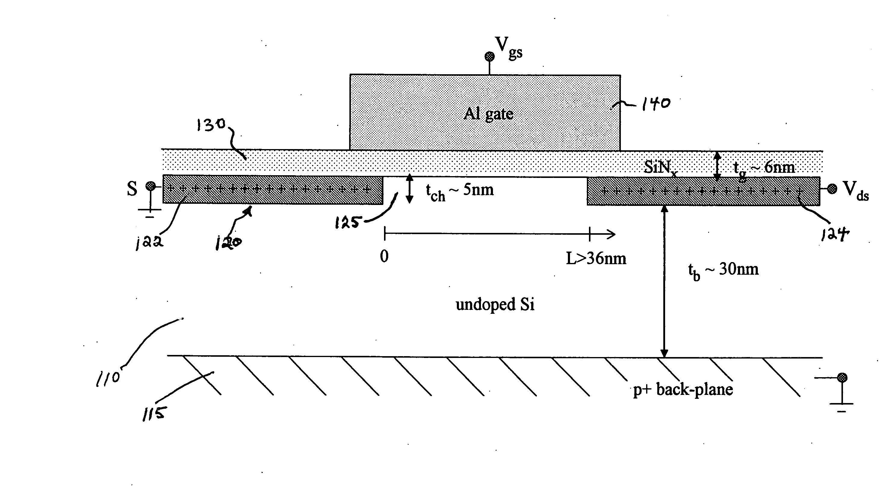
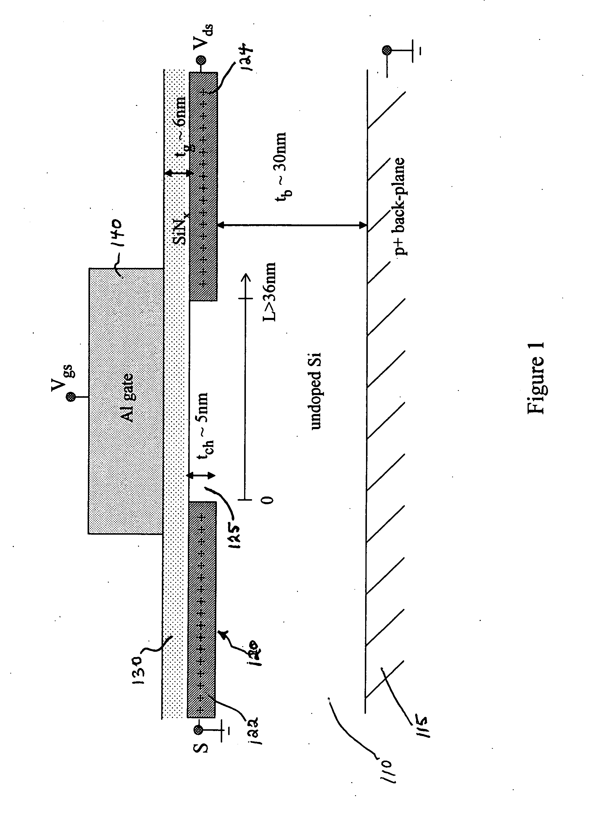
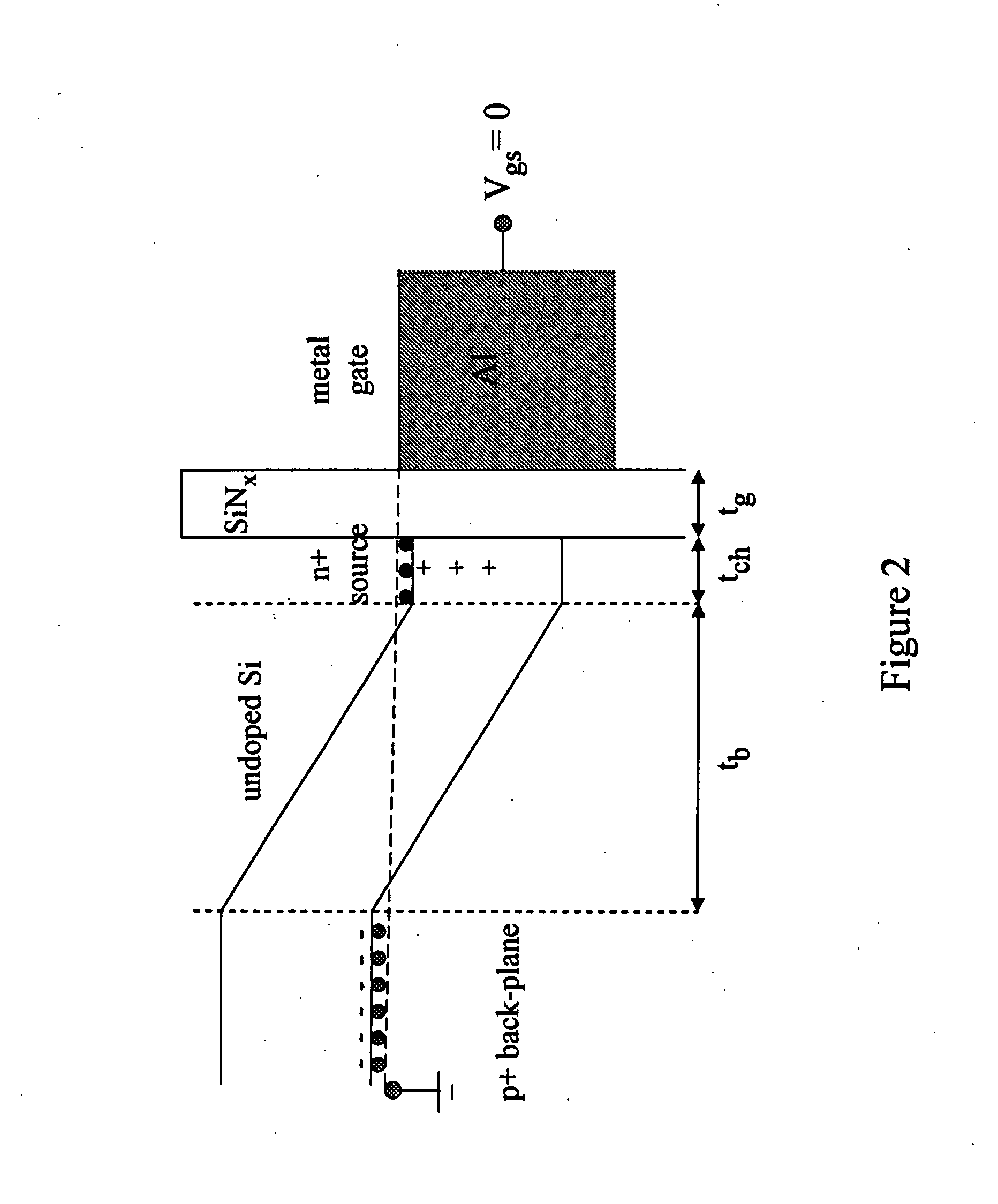
[0032]FIG. 1 illustrates a principle of the invention by showing an embodiment of a field-effect transistor device which has the source, drain, channel, and associated “wiring” (e.g., terminal couplings to source and drain) fabricated by patterning an ultra dense delta-doped layer within an epitaxially deposited semiconductor layer. In this simplified embodiment, an undoped silicon body 110 has a p+ back-plane 115 on its bottom surface. The epitaxially deposited layer 120 has, in this example, about 2.5 nm of Si on which is deposited, in patterned source (122) and drain (124) regions of the plane, ultra dense delta-doped layers of, in this example, n+ dopant, overgrown by another ˜2.5 nm of Si. Accordingly, the layer 120, in this embodiment, has a thickness of ˜5 nm, as seen at the channel region 125, with tch being about 5 nm. The channel length, L, in this example, is about 36 nm. Also, in this simplified embodiment, a gate insulator layer (130) of about 6 nm of SiNx is grown over...
PUM
 Abstract
Description
Claims
Application Information