

Method of manufacturing nitride semiconductor light-emitting element and nitride semiconductor light-emitting element
a technology of nitride semiconductor and light-emitting element, which is applied in the direction of basic electric elements, semiconductor devices, electrical equipment, etc., can solve the problems of property degradation of nitride semiconductor light-emitting element, distorted active layer during formation of unevenness, etc., to achieve the effect of improving light extraction efficiency and suppressing the degradation of an active layer
- Summary
- Abstract
- Description
- Claims
- Application Information
AI Technical Summary
Benefits of technology
Problems solved by technology
Method used
Image

Examples
example 1
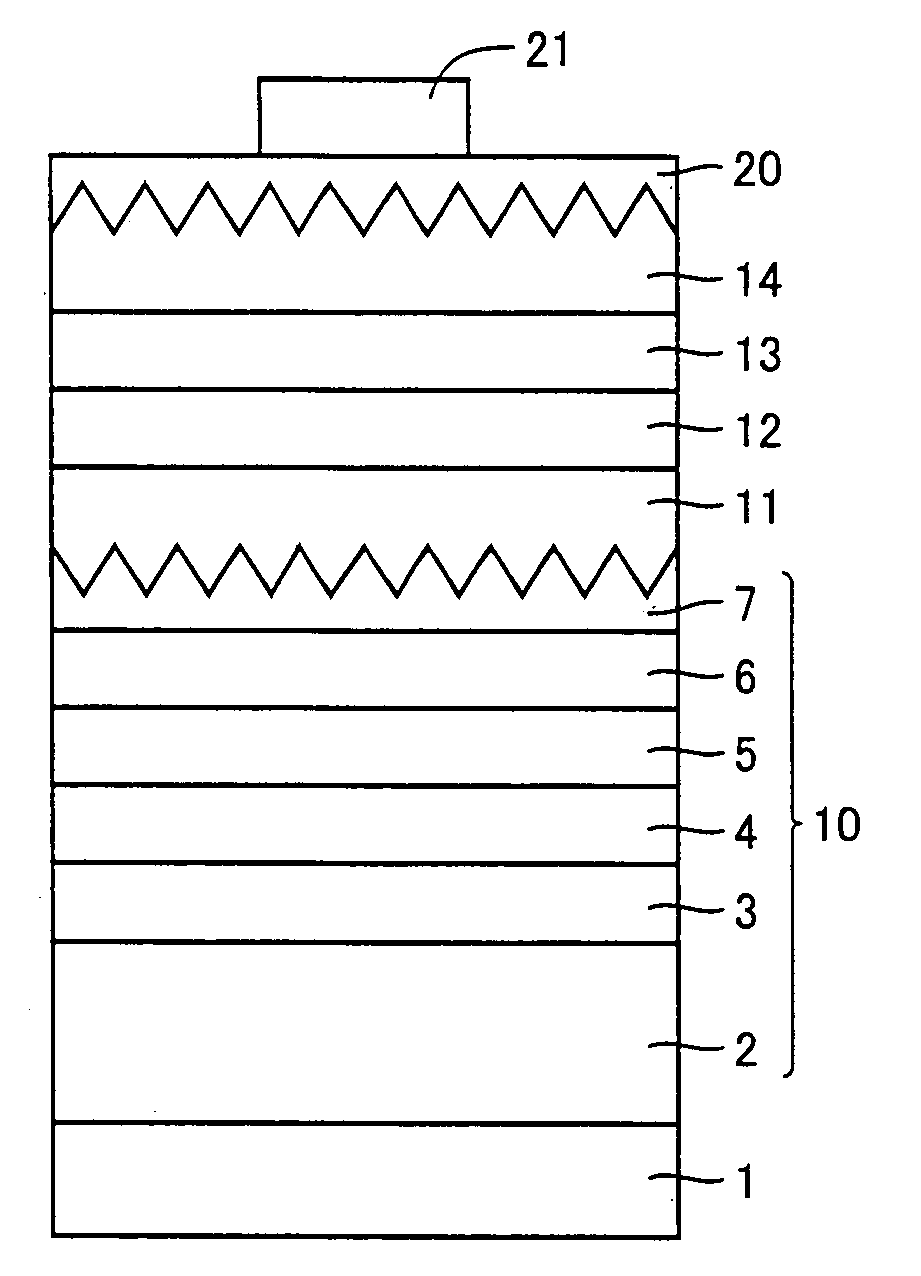
[0062]Initially, a sapphire substrate was prepared as a substrate, and a mask layer made of a silicon nitride layer was formed on a surface (C+ plane) of the sapphire substrate. Next, a photolithography technique and a hydrofluoric acid etchant were used to remove a portion of the mask layer, so as to leave the mask layer in the form of stripes, each extending in approximately parallel with of the sapphire substrate and having a width of approximately 3 μm, and expose the surface of the sapphire substrate in the form of stripes, each having a width of 2 μm.
[0063]Subsequently, an exposed portion of the surface of the sapphire substrate was etched by RIE to a depth of approximately 0.5 μm, to form unevenness at the surface of the sapphire substrate. The sapphire substrate having the unevenness formed at its surface was then placed in an MOCVD device, and the sapphire substrate was heated to a temperature of 1100° C. to clean the surface thereof. Subsequently, trimethylaluminum (TMA),...
PUM
| Property | Measurement | Unit |
|---|---|---|
| temperature | aaaaa | aaaaa |
| width | aaaaa | aaaaa |
| width | aaaaa | aaaaa |
Abstract
Description
Claims
Application Information