Mold for forming conductive bump, method of fabricating the mold, and method of forming bump on wafer using the mold

a mold and conductive technology, applied in the field of molds for forming conductive bumps, can solve the problems of limited types of components that form solder bumps, low manufacturing speed, and large distance between bumps, and achieve the effect of high mold precision

Active Publication Date: 2007-12-20
SAMSUNG ELECTRONICS CO LTD
View PDF0 Cites 11 Cited by
  • Summary
  • Abstract
  • Description
  • Claims
  • Application Information

AI Technical Summary

Benefits of technology

[0012]Some embodiments of the present invention provide a mold for forming a conductive bump, a method of fabricating the mold, and a method of forming a bump on a wafer using the mold. Some embodiments of the present invention enable the bump to be formed by employing various materials, the mold to be repeatedly used several times because the mold is not damaged in the method, and due to a high precision of the mold, the bump pitch is not limited.

Problems solved by technology

An advantage of the solder ball placement method is that the uniformity of the heights of the solder bumps, after reflow, can be easily controlled, but drawbacks are that manufacturing speed is significantly low compared to that of the electroplating or stencil printing method, and the distance between bumps must be very wide to accommodate the solder ball placement equipment.
When the electroplating method or the evaporation method is used, the types of component elements that form the solder bump are limited.
That is, the solder bumps are difficult to fabricate when three metal elements or more are used in the electroplating method or the evaporation method.
Further, since high-cost processes such as a photolithography process must be performed, fabrication costs increase.
The stencil printing method has an advantage that the bump fabrication facilities are relatively simple and low-priced, but it is limited in that the quality of the bump formed on a wafer depends on the physical properties of the printed solder paste, specifically, the mixture of solder powder and flux, and the fabrication capabilities of the stencil.
In particular, as the size of a wafer increases, the integration density of semiconductor chips increases, and the number of pins increases, the stencil printing method becomes more limited in its ability to accomplish a required fine pitch and achieve coplanarity of the heights of the reflowed solder bumps.
Further, methods containing intermediate formation processes also have drawbacks in that continuous use may be limited because a substrate where a solder bump is formed may be damaged or worn by cleaning or by the pressure applied during the transfer of the solder bump to a semiconductor wafer.

Method used


Image

  • Mold for forming conductive bump, method of fabricating the mold, and method of forming bump on wafer using the mold
  • Mold for forming conductive bump, method of fabricating the mold, and method of forming bump on wafer using the mold
  • Mold for forming conductive bump, method of fabricating the mold, and method of forming bump on wafer using the mold

Examples


first embodiment

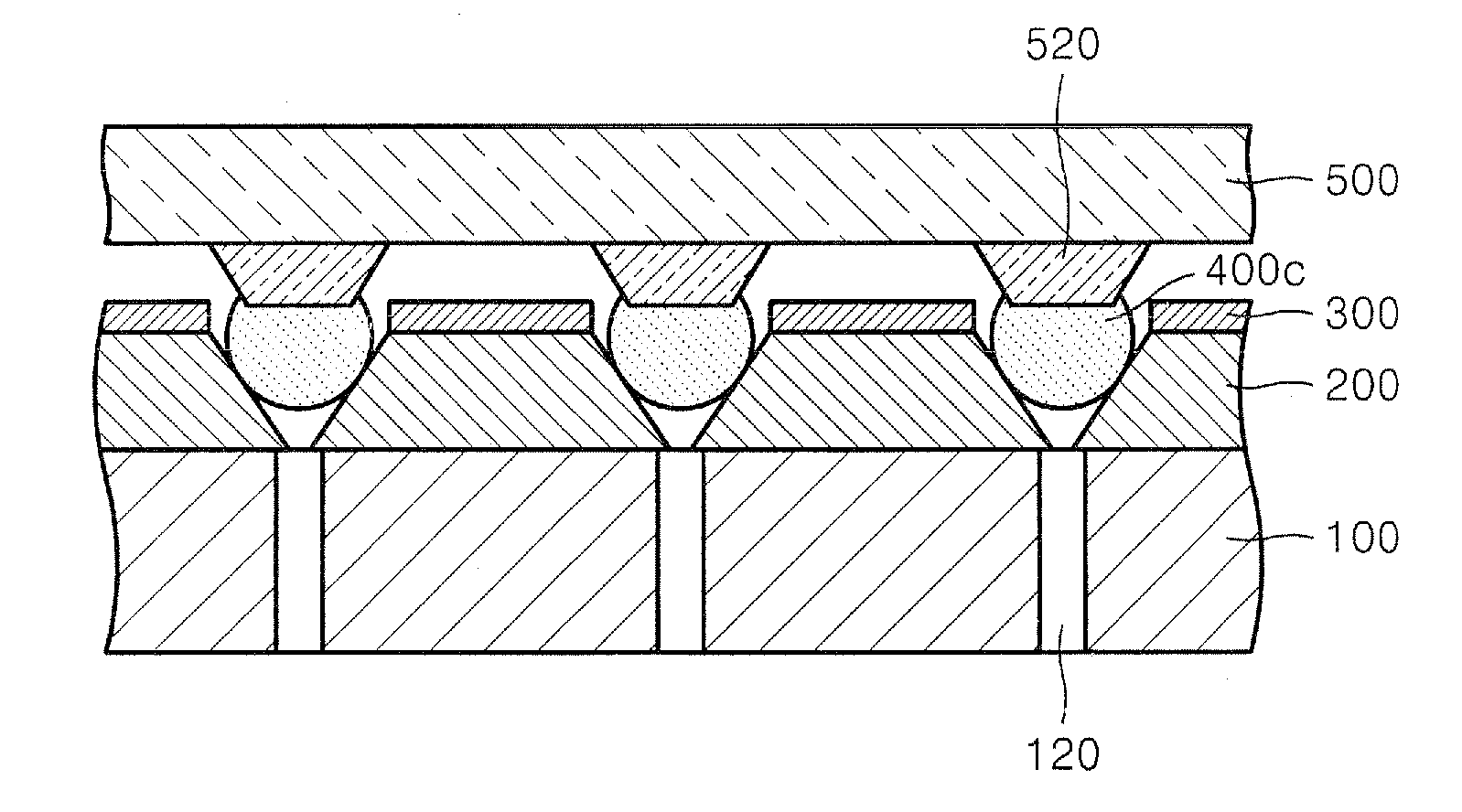
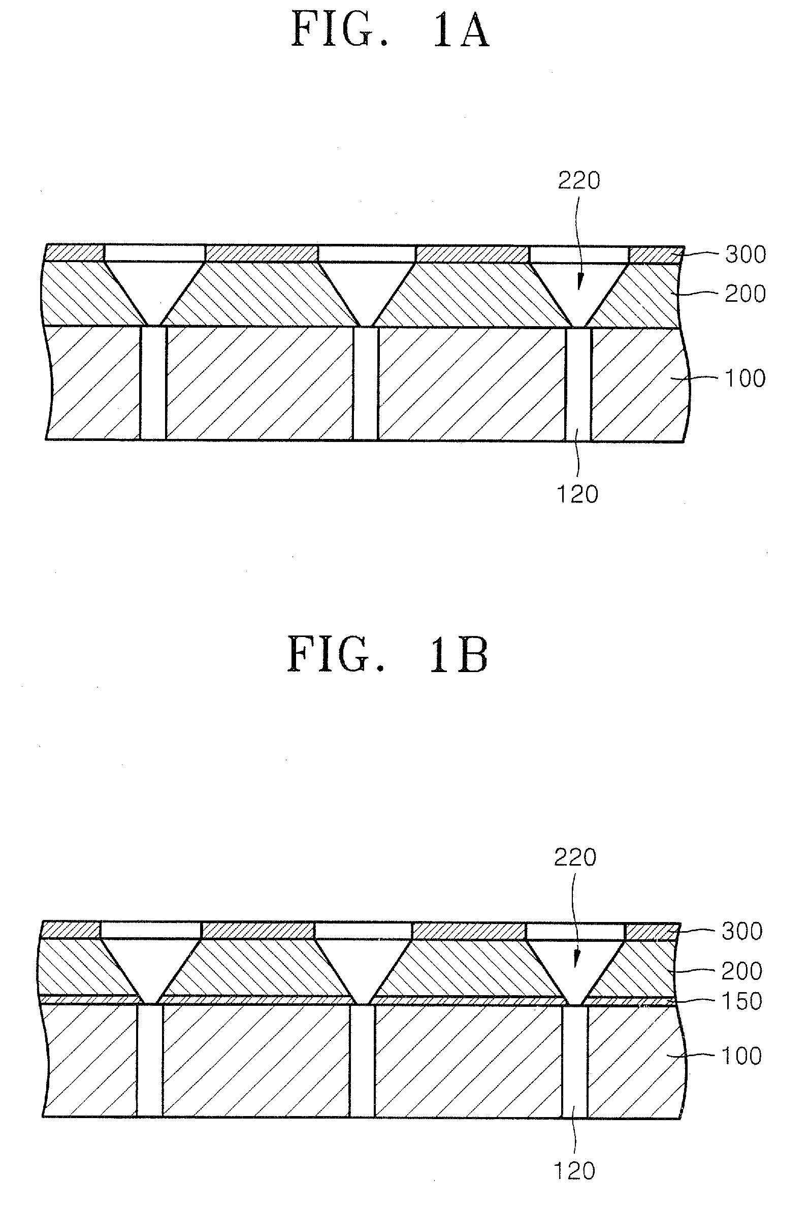
[0022]FIG. 1A is a cross-sectional view illustrating a mold for forming a conductive bump according to the present invention.

[0023]Referring to FIG. 1A, a mold for forming a conductive bump according to an embodiment of the present invention includes a first substrate 200 having a plurality of grooves 220, a second substrate 100 formed below the first substrate and having through-holes 120 respectively in communication with the bottoms of the grooves 220, and a mask layer 300 with a pattern on the first substrate 200. The plurality of grooves may have, for example, a substantially funnel-shape, among other shapes as discussed below.

[0024]The mold for forming a conductive bump according to an embodiment of the present invention may have a three-layered structure including the first and second substrates 200 and 100, and the mask layer 300. However, the present invention is not limited to the three-layered structure, but the mold may have a structure with a greater number of layers, i...

second embodiment

[0030]FIG. 1B is a sectional view illustrating a mold for forming a conductive bump according to the present invention.

[0031]Referring to FIG. 1B, the mold for forming a conductive bump according to the second embodiment is similar to the mold for forming a conductive bump in the embodiment of FIG. 1A, but an adhesive layer 150 is formed between a first substrate 200 and a second substrate 100 to bond the first and second substrates 200, 100. Thus, since the mold for forming a conductive bump according to this embodiment further comprises the adhesive layer 150, it has a four-layered structure unlike the embodiment of FIG. 1A. However, the mold for forming a conductive bump according to this embodiment may have a structure having a greater number of layers, if necessary.

[0032]The first substrate 200 and the second substrate 100 may be attached to each other using various bonding methods. For example, an anodic bonding method applying a high voltage at an appropriate temperature, or ...

fourth embodiment

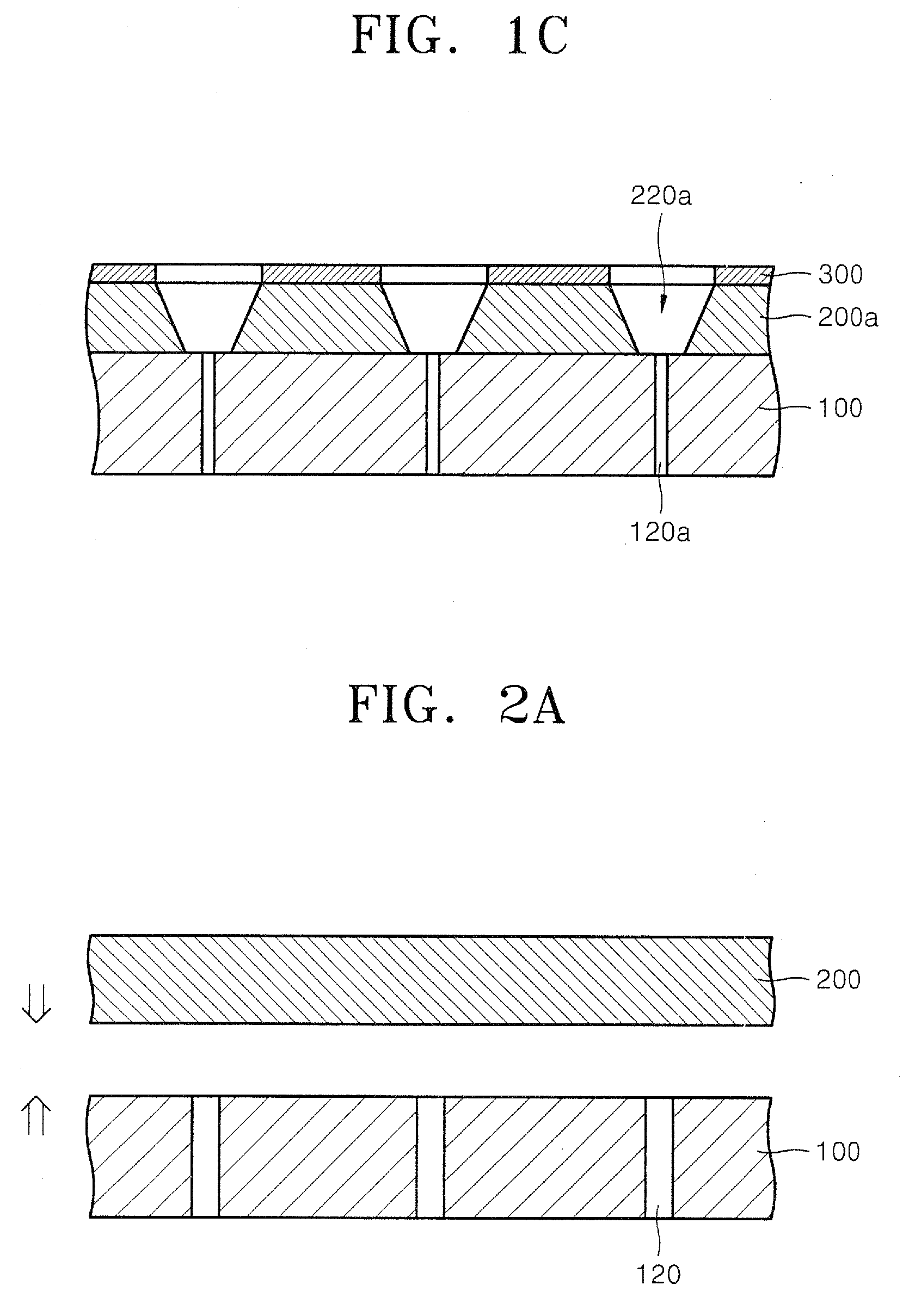
[0058]FIG. 4 is a sectional view illustrating a mold for forming a conductive bump used in a method of forming a bump on a wafer according to the present invention.

[0059]Referring to FIG. 4, the method of forming a bump on a wafer according to an embodiment of the present invention can be accomplished using a mold without a second substrate having a through-hole. However, since vacuum adsorption cannot be used during the method, the removal of a conductive powder is preferably performed using a blade.

[0060]Meanwhile, since the shape of the groove 220 of the first substrate 200a is not limited to a funnel shape, various shapes of the groove can be used.

[0061]As described above, the mold for forming a conductive bump according to an embodiment of the present invention overcomes the problems caused in the methods of forming a bump using an electroplating process, an evaporation process, and a printing method.

[0062]Further, various shapes of a mold for forming a conductive bump can be e...


PUM

PropertyMeasurementUnit
thicknessaaaaaaaaaa
diameteraaaaaaaaaa
diameteraaaaaaaaaa

Abstract

A mold for forming a conductive bump, a method of fabricating the mold, and a method of forming a bump on a wafer using the mold are provided. The bump can be formed by employing various materials, the mold can be repeatedly used several times because the mold is not damaged, and due to a high precision, the pitch of the bumps is not limited. The mold for forming a conductive bump comprises a first substrate having a groove to form a bump; a second substrate for vacuum adsorption formed below the first substrate, and having a through-hole in communication with the groove; and a mask layer formed on the first substrate, and used to form the groove.

Description

CROSS-REFERENCE TO RELATED PATENT APPLICATION[0001]This application claims priority from Korean Patent Application No. 10-2006-0054923, filed on Jun. 19, 2006, in the Korean Intellectual Property Office, the disclosure of which is incorporated herein in its entirety by reference.BACKGROUND[0002]1. Technical Field[0003]The present invention relates to a semiconductor device and a method of fabricating the same, and more particularly, to a mold for forming a conductive bump used in connecting interconnections of a semiconductor device, a method of fabricating the mold, and a method of forming a bump on a semiconductor wafer using the mold.[0004]2. Description of the Related Art[0005]Micro devices such as a semiconductor device or a micro electro mechanical system (MEMS) normally use a wire bonding method, a taped automated bonding (TAB) method, a flip chip method or the like in order to electrically connect chips to an external substrate such as a printed circuit board (PCB).[0006]The...

Claims


Application Information

Patent Timeline
Patent Type & Authority Applications(United States)
IPC IPC(8): H01L23/48
CPCH01L24/11H01L2224/13099H01L2224/11334H01L2924/014H01L2924/01033H01L24/05H01L2224/05556H01L2224/05568H01L2224/05573H01L2924/00014H01L2924/181H01L2924/00H01L2224/05599H01L21/52
Inventor HWANG, TAE-JOO
Owner SAMSUNG ELECTRONICS CO LTD
Why Eureka
Try Eureka