Artificial dielectrics using nanostructures

a technology of nanostructures and dielectrics, applied in the field of nanowires, can solve the problems of limited application and use of existing artificial dielectrics, limited dielectric structures based on existing dielectrics, and limited dielectric structures in their application, so as to improve the performance of cell phones and improve the ram and other coatings for stealth operation.

Inactive Publication Date: 2007-12-27
NANOSYS INC
View PDF51 Cites 13 Cited by
  • Summary
  • Abstract
  • Description
  • Claims
  • Application Information

AI Technical Summary

Benefits of technology

[0025] Artificial dielectrics using nanostructures within electronic devices can be used to improve the performance of cell phones, wireless personal digital assistants, 802.11 PC cards, global positioning satellites (GPS) receivers, and essentially any other apparatus that either receives or transmits radio waves. Furthermore, artificial dielectrics, and in particular, controllable dielectric materials using nanostructures can be used to significantly improve RAM and other coatings for stealth operation.

Problems solved by technology

Existing artificial dielectrics are limited in their application and use because they typically have relatively low dielectric constants and have fixed dielectric constants at a particular frequency.
These limitations, as discussed in Stockton, have been attributed to clumping of metallized fibers once the density of the fibers becomes high.
When the metallized fibers clump, they lose their insulative characteristics and become conducting, thereby limiting the ability to achieve high dielectric constants within existing artificial dielectrics.
Furthermore, dielectric structures based on existing dielectrics and dielectric structures are limited in their application.

Method used


Image

  • Artificial dielectrics using nanostructures
  • Artificial dielectrics using nanostructures
  • Artificial dielectrics using nanostructures

Examples


Embodiment Construction

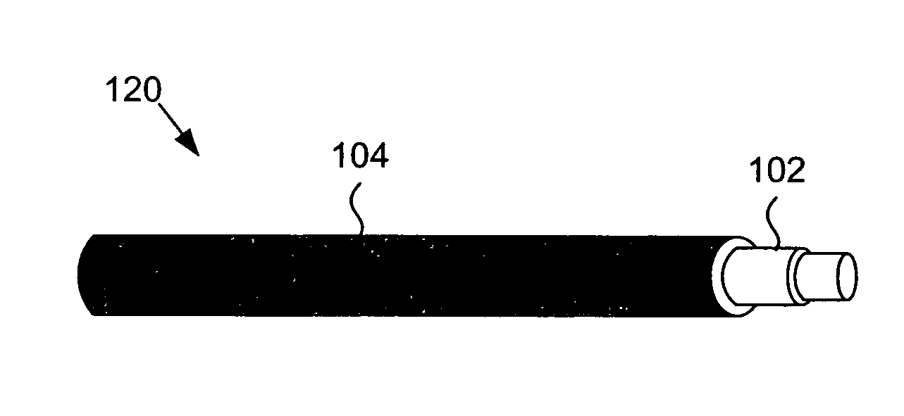
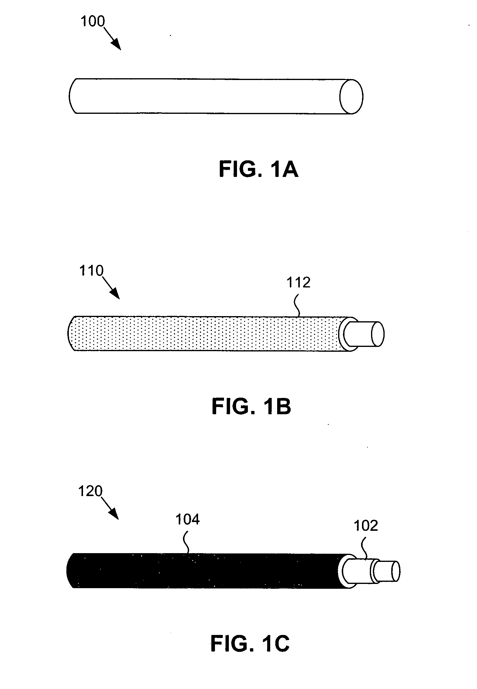
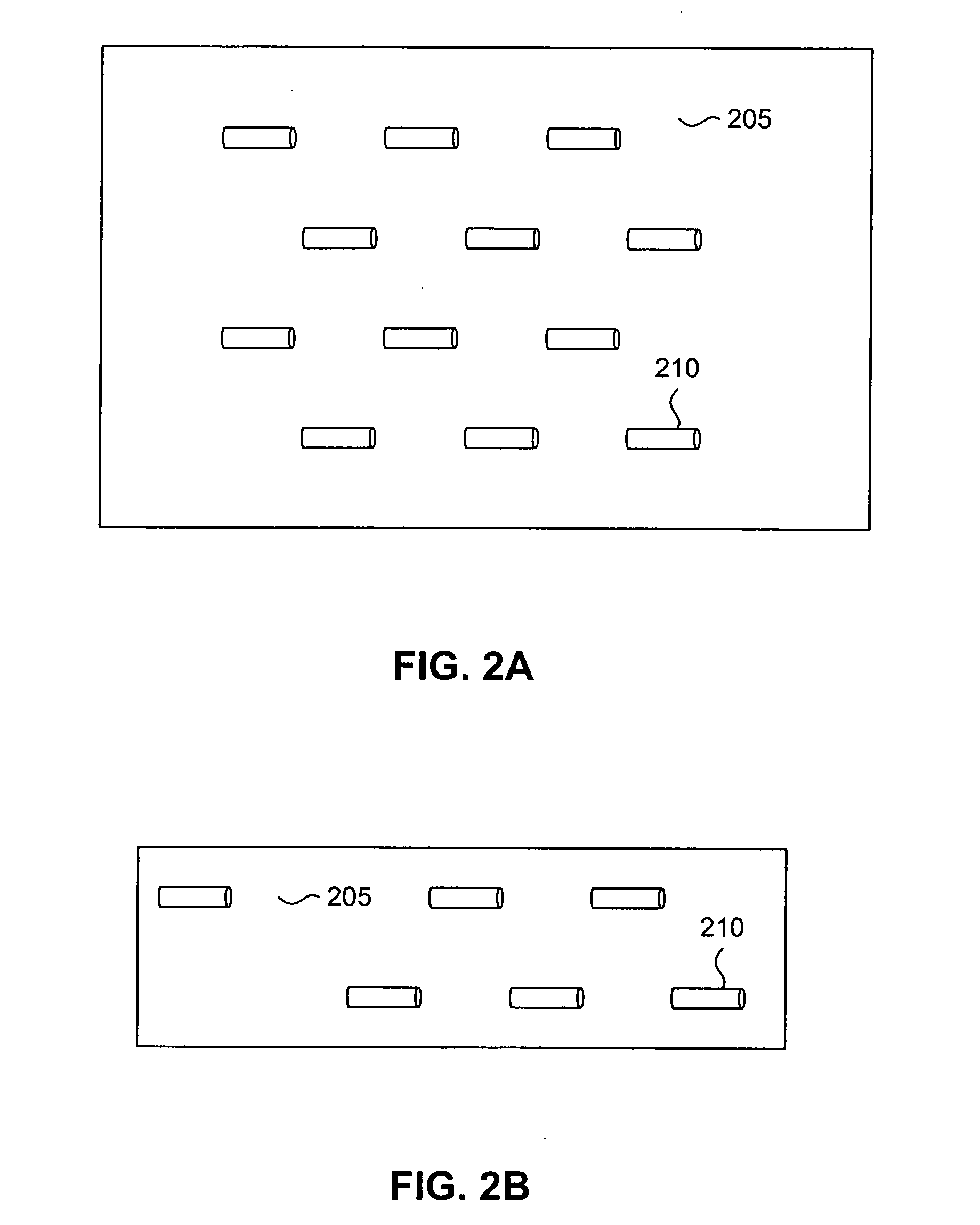
[0052] It should be appreciated that the particular implementations shown and described herein are examples of the invention and are not intended to otherwise limit the scope of the present invention in any way. Indeed, for the sake of brevity, conventional electronics, manufacturing, semiconductor devices, and nanowire (NW), nanorod, nanotube, and nanoribbon technologies and other functional aspects of the systems (and components of the individual operating components of the systems) may not be described in detail herein. Furthermore, for purposes of brevity, the invention is frequently described herein as pertaining to nanowires, and to a semiconductor diode device.

[0053] Moreover, while a single nanowire is illustrated for the specific implementations discussed, the implementations are not intended to be limiting and a wide range of the number of nanowires and spacing can also be used. It should be appreciated that although nanowires are frequently referred to, the techniques de...


PUM

PropertyMeasurementUnit
dielectric constantsaaaaaaaaaa
lengthaaaaaaaaaa

Abstract

Artificial dielectrics using nanostructures, such as nanowires, are disclosed. In embodiments, artificial dielectrics using other nanostructures, such as nanorods, nanotubes or nanoribbons and the like are disclosed. The artificial dielectric includes a dielectric material with a plurality of nanowires (or other nanostructures) embedded within the dielectric material. Very high dielectric constants can be achieved with an artificial dielectric using nanostructures. The dielectric constant can be adjusted by varying the length, diameter, carrier density, shape, aspect ratio, orientation and density of the nanostructures. Additionally, a controllable artificial dielectric using nanostructures, such as nanowires, is disclosed in which the dielectric constant can be dynamically adjusted by applying an electric field to the controllable artificial dielectric. A wide range of electronic devices can use artificial dielectrics with nanostructures to improve performance. Example devices include, capacitors, thin film transistors, other types of thin film electronic devices, microstrip devices, surface acoustic wave (SAW) filters, other types of filters, and radar attenuating materials

Description

CROSS REFERENCE TO RELATED APPLICATIONS [0001] The present application claims priority to U.S. Provisional Patent Application No. 60 / 610,219, entitled Artificial Dielectrics Using Nanostructures, filed on Sep. 16, 2004 by Stumbo et. al., which is hereby expressly incorporated by reference in its entirety.STATEMENT REGARDING FEDERALLY-SPONSORED RESEARCH AND DEVELOPMENT [0002] Not applicable. BACKGROUND OF THE INVENTION [0003] 1. Field of the Invention [0004] The invention relates to nanowires, and more particularly to controllable artificial dielectrics using nanowires. [0005] 2. Background Art [0006] Dielectrics are materials that are used primarily to isolate components electrically from each other or to act as capacitive elements in devices, circuits and systems. A unique characteristic of a dielectric is that nearly all or a portion of the energy required for its charging from an external electrical field can be recovered when the field is removed. Dielectrics have an extremely w...

Claims


Application Information

Patent Timeline
Patent Type & Authority Applications(United States)
IPC IPC(8): H01L27/12
CPCB82Y10/00B82Y30/00G11C2213/16G11C2213/81H01L29/0665H01L29/0673Y10S977/743H01L51/0537Y10S977/762Y10S977/936Y10S977/813Y10S977/745H01L29/4908H10K10/478H01B3/00B82B3/00
Inventor STUMBO, DAVID P.EMPEDOCLES, STEPHEN A.LEON, FRANCISCOPARCE, J. WALLACE
Owner NANOSYS INC
Why Eureka
Try Eureka