

Variable-gain amplifier
- Summary
- Abstract
- Description
- Claims
- Application Information
AI Technical Summary
Benefits of technology
Problems solved by technology
Method used
Image

Examples
first embodiment
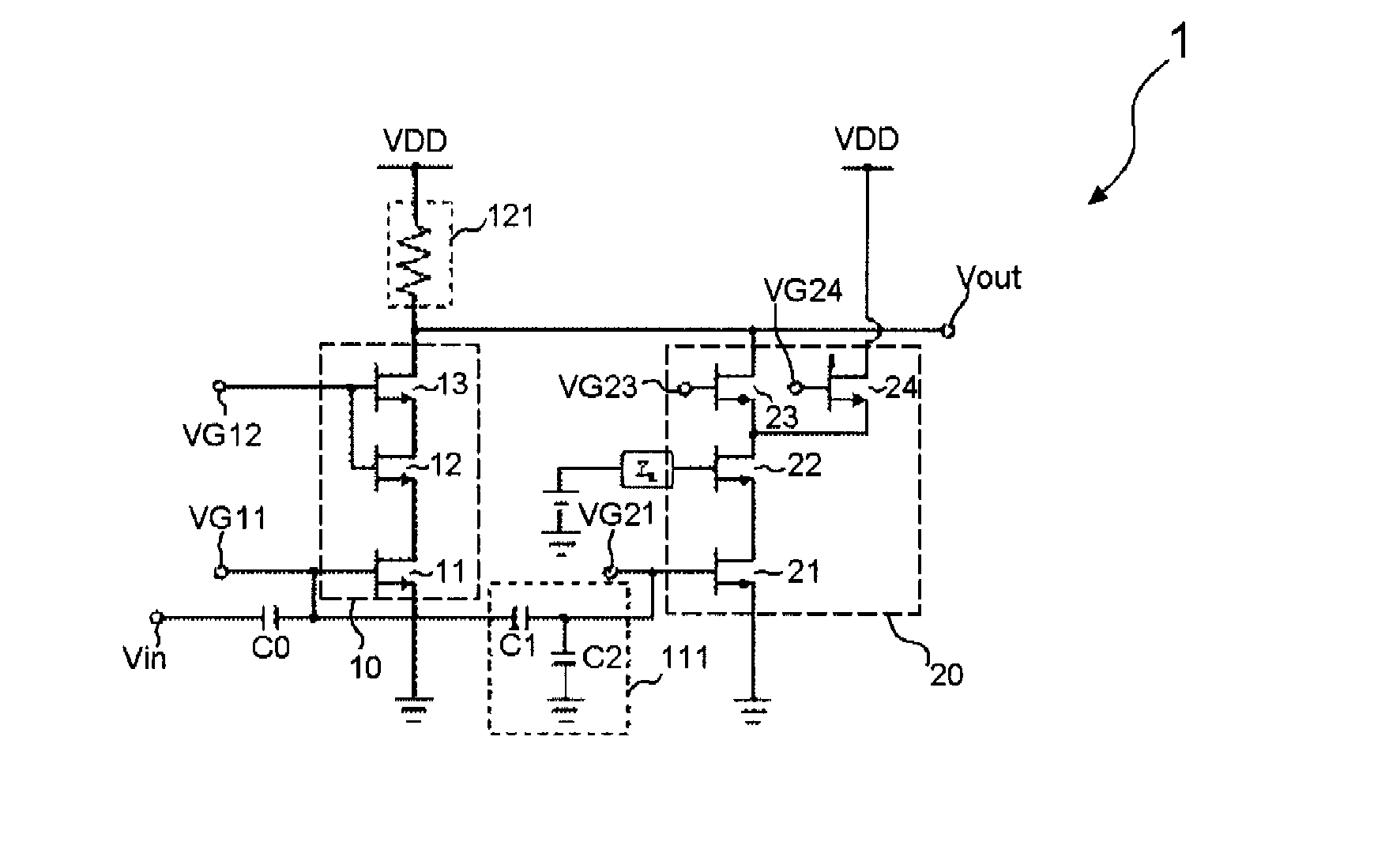
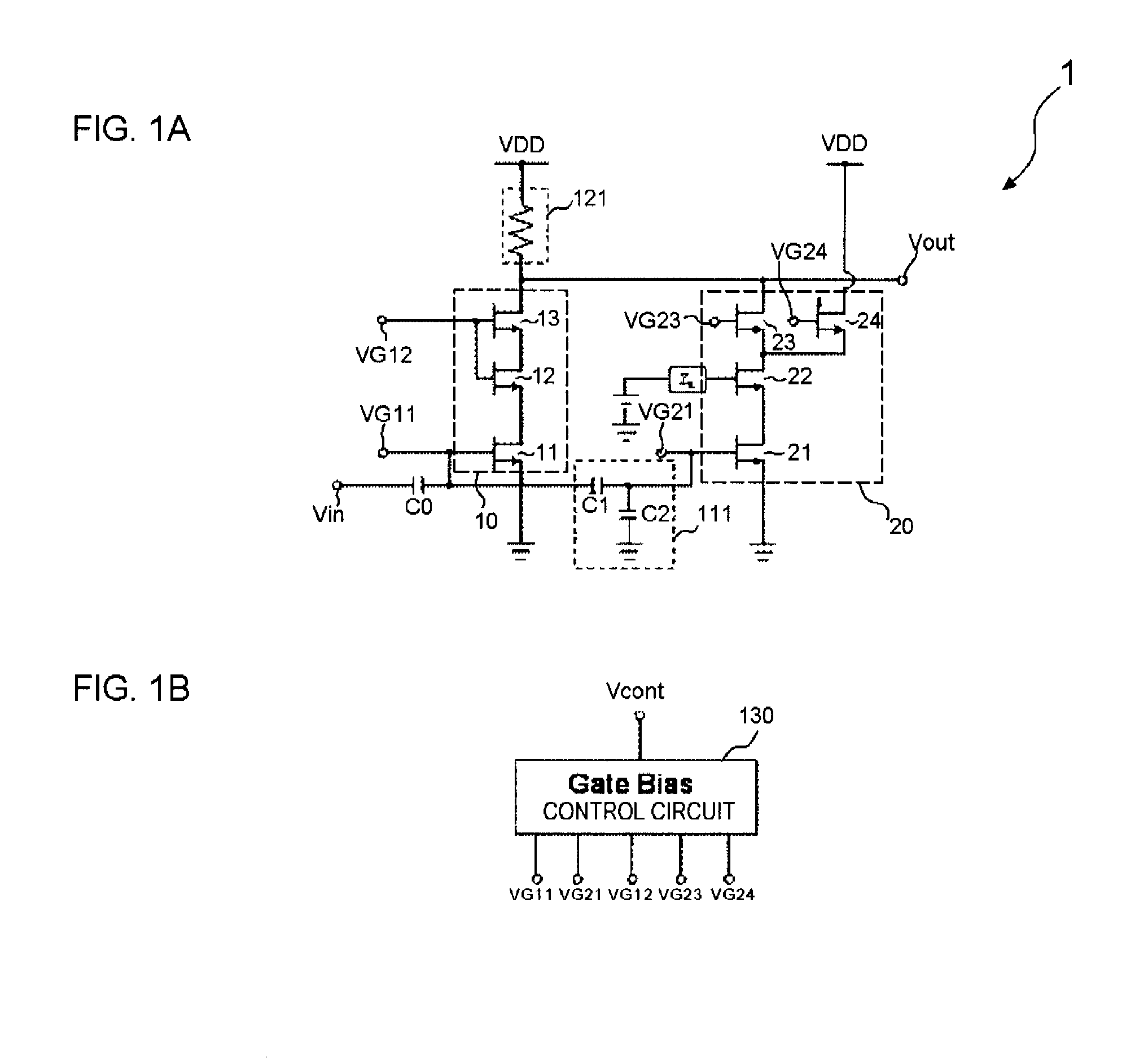
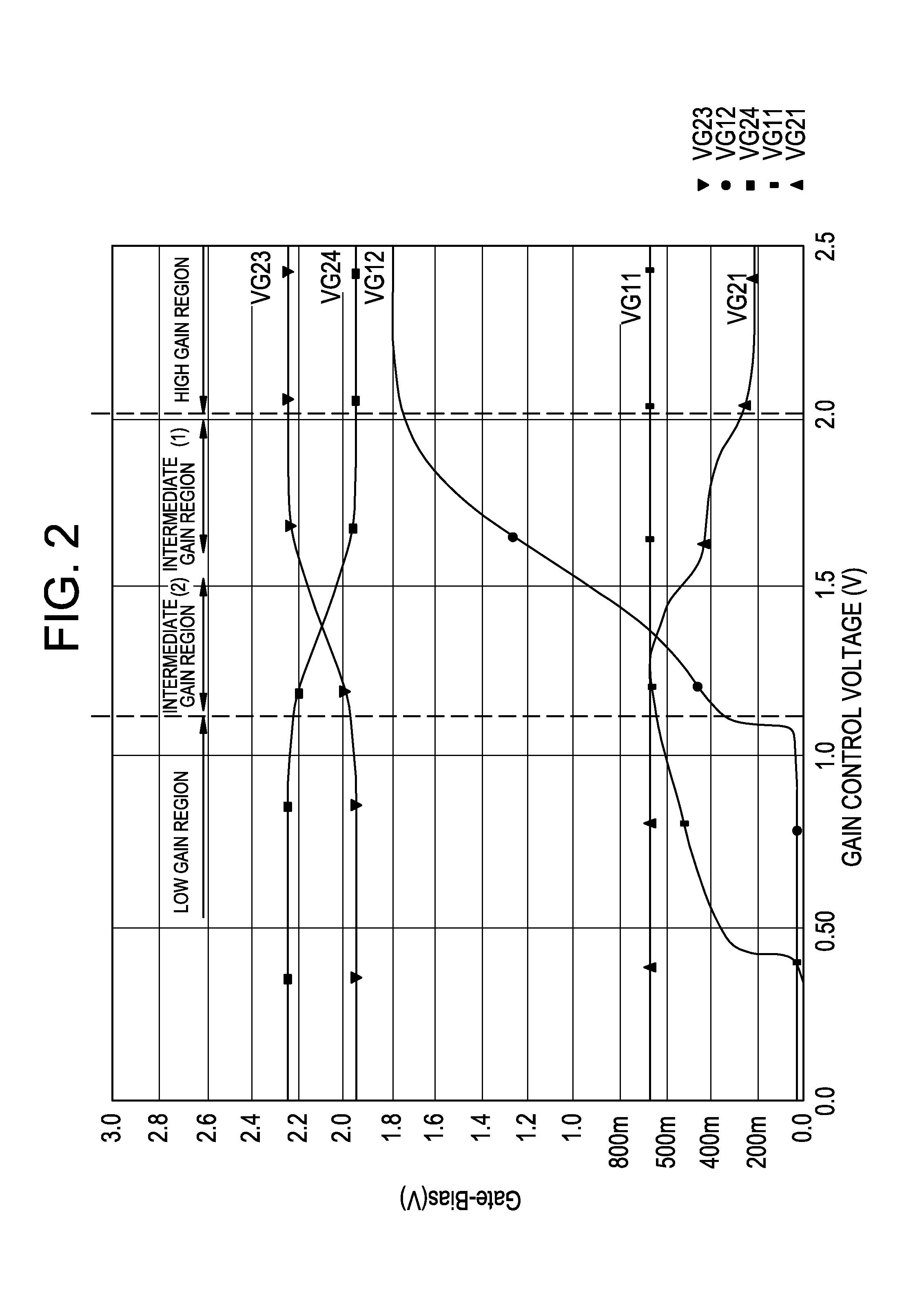
[0039]FIG. 1A is a circuit diagram of a variable-gain amplifier according to a first embodiment of the present invention. The variable-gain amplifier 1 includes n pieces of cascode amplifiers 10, 20, and an attenuator 111. n represents an integer not fewer than 2, and in this embodiment n is 2. The cascode amplifiers 10, 20 are mutually connected in parallel, via the attenuator 111.
[0040] The first cascode amplifier 10 is connected to an input terminal Vin of the variable-gain amplifier 1 via a capacitor C0. The second cascode amplifier 20 is connected to the input terminal Vin via the capacitor C0 and the attenuator 111. The attenuator 111 includes a capacitor C1 and a capacitor C2. The capacitor C1 is provided on a signal path between the input terminal Vin and the cascode amplifier 20. The capacitor C2 is provided between a signal path between the capacitor CT and the cascode amplifier 20, and the ground.
[0041] Each of the cascode amplifiers 10, 20 includes a plurality of casco...
second embodiment
[0073]FIG. 8 is a circuit diagram of a variable-gain amplifier according to a second embodiment of the present invention. The variable-gain amplifier 2 includes three cascode amplifiers 30, 40, 50, and two attenuators 112, 113. The cascode amplifiers 30, 40, 50 are mutually connected in parallel, via the attenuators 112, 113. More specifically, the attenuator 112 is interposed between the cascode amplifier 30 and the cascode amplifier 40, and the attenuator 113 is interposed between the cascode amplifier 40 and the cascode amplifier 50.
[0074] The cascode amplifier 30 and the cascode amplifier 40 have a similar circuit configuration to that of the cascode amplifier 10 in FIG. 1. In other words, FETs 31, 41 correspond to the FET 11 of the cascode amplifier 10, FETs 32, 42 to the FET 12, and FETs 33, 43 to the FET 13. The cascode amplifier 50 has a similar circuit configuration to that of the cascode amplifier 20 in FIG. 1. In other words, FETs 51, 52, 53, 54 respectively correspond t...
third embodiment
[0079]FIG. 9 is a circuit diagram of a variable-gain amplifier according to a third embodiment of the present invention. The variable-gain amplifier 3 includes cascode amplifiers 60, 70, and an attenuator 114. The cascode amplifiers 60, 70 are mutually connected in parallel via the attenuator 114.
[0080] The cascode amplifier 60 includes FETs 61 to 66. The FETs 61, 63, 65 are cascode-connected in a similar manner to the FETs 11, 12, 13 in FIG. 1. The gate of the FET 61 is connected to a non-inverted input terminal Vin+. The drain of the FET 65 is connected to a load 122.
[0081] The FETs 62, 64, 66 are also cascode-connected in a similar manner to the FETs 11, 12, 13 in FIG. 1. The gate of the FET 62 is connected to an inverted input terminal Vin−. The drain of the FET 66 is connected to a load 123.
[0082] The cascode amplifier 70 includes FETs 71 to 78. The FETs 71, 73, 75 are cascode-connected in a similar manner to the FETs 21, 22, 23 in FIG. 1. The FET 77 has the source connected...
PUM
 Abstract
Description
Claims
Application Information