Liquid crystal display device and method of driving the same

a display device and liquid crystal technology, applied in static indicating devices, non-linear optics, instruments, etc., can solve problems such as image persistence, liquid crystal deterioration, and increase power consumption, and achieve low power consumption, improve the holding characteristics of active elements, and improve the effect of circuit siz

Inactive Publication Date: 2007-12-27
MITSUBISHI ELECTRIC CORP
View PDF10 Cites 33 Cited by
  • Summary
  • Abstract
  • Description
  • Claims
  • Application Information

AI Technical Summary

Benefits of technology

[0016]It is an object of the present invention to provide a liquid crystal display device capable of improving the holding characteristics of an active element during a vertical blanking interval with low power consumption and without increasing the circuit size, and a method of driving the same.

Problems solved by technology

As well known, a liquid crystal deteriorates upon being kept applied with DC voltage, resulting in a fault such as image persistence.
The above problem is caused by not only the TFT leakage but parasitic capacitance CDS across the drain and source.
Thus a pixel potential influenced by the potential of the last row is held during the vertical blanking interval, resulting in the same problem as described above.
The above problem causes a difference in shade between the pixels A and B, and also causes an effective DC component to be applied to the liquid crystal, which leads to liquid crystal deterioration.
In a liquid crystal display device with the low frame frequency driving system, a blanking interval is significantly extended, which further encourages the above problem.
This method, however, increases power consumption because the source lines need to be driven during the vertical blanking interval when they do not originally need to be driven.
The method disclosed in JP 5-313607 thus cannot be adopted for a liquid crystal display device with the low frame frequency driving system for low power consumption.
Yet this method requires a separate charging circuit which increases the circuit size.

Method used


Image

  • Liquid crystal display device and method of driving the same
  • Liquid crystal display device and method of driving the same
  • Liquid crystal display device and method of driving the same

Examples


first preferred embodiment

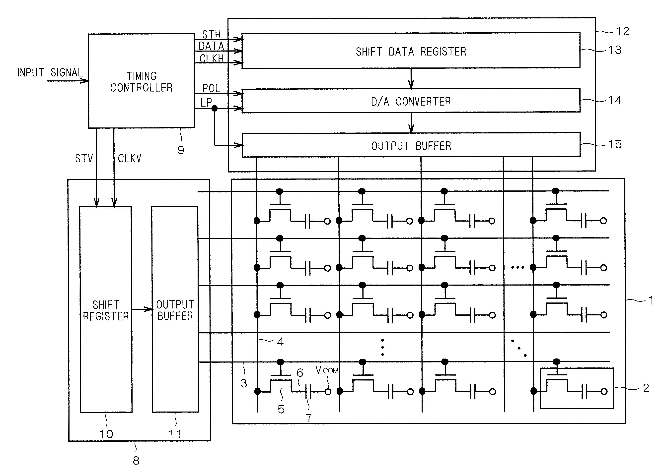
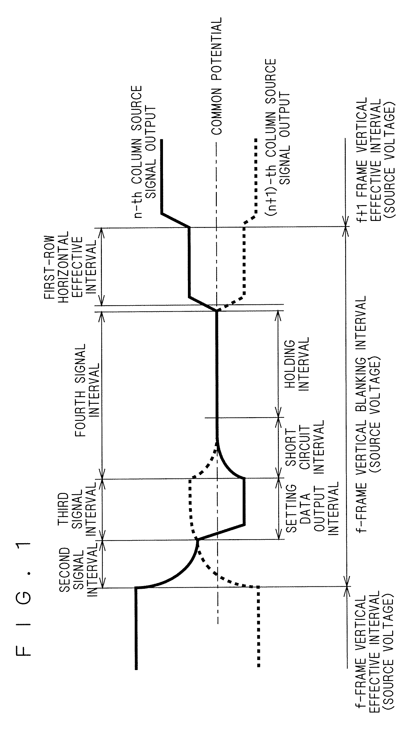
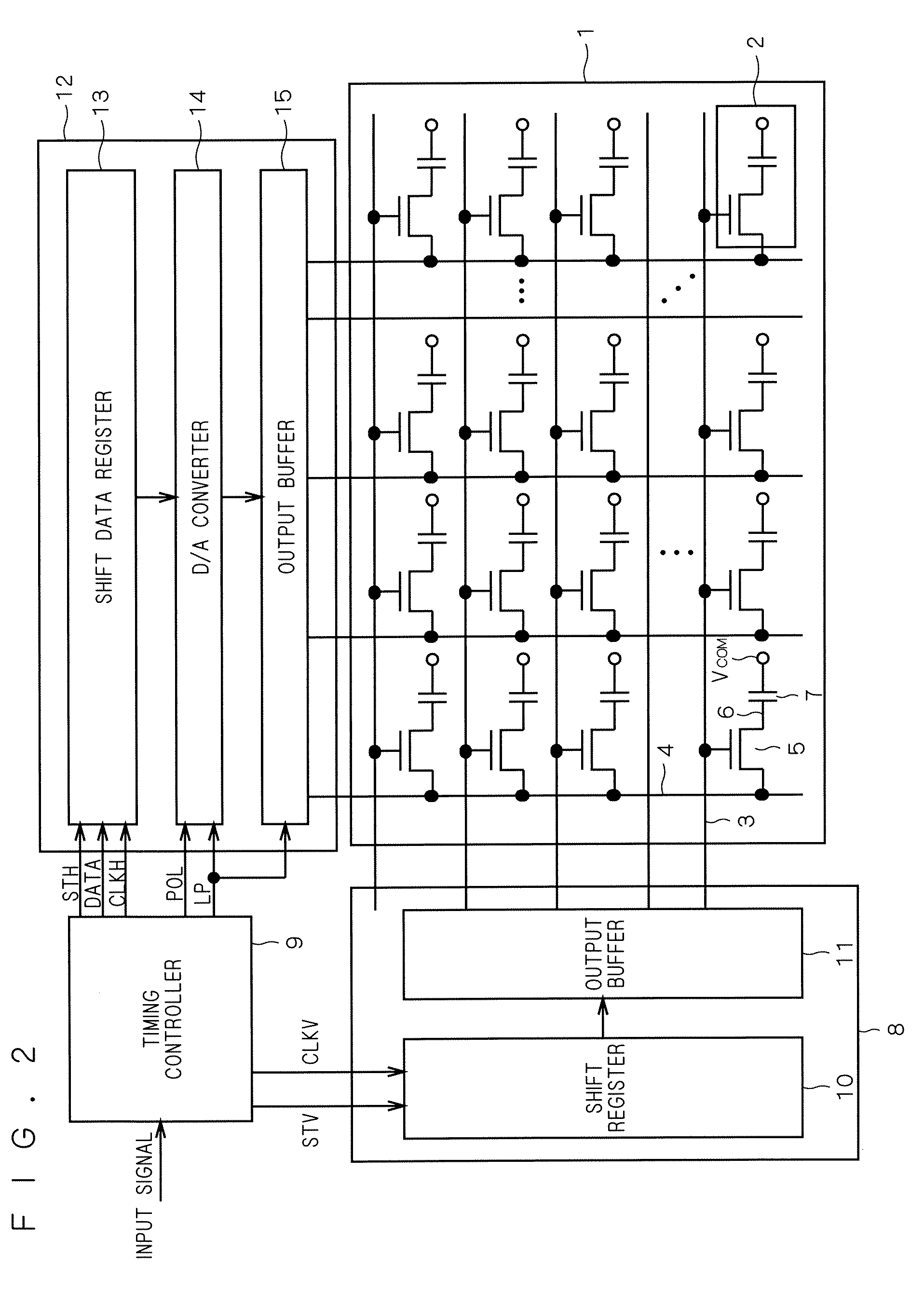
[0033]FIG. 1 shows potential variations in source line of a liquid crystal display device according to a first preferred embodiment. FIG. 2 is a block diagram of the liquid crystal display device according to this embodiment. Referring to FIG. 2, the structure of the liquid crystal display device according to this embodiment is first described. The structure of a typical active matrix TFT liquid crystal display device may be used for the liquid crystal display device according to this embodiment.

[0034]The liquid crystal display device shown in FIG. 2 has pixels 2 arranged in a matrix on a translucent substrate 1, and gate lines 3 and source lines 4 interconnected to surround the pixels 2. Provided at the intersection of each gate line 3 and each source line 4 is a thin film transistor (TFT 5), an active element, whose drain electrode 6 is connected to a pixel element. An opposed substrate (not shown) is provided in an opposed position to the substrate 1 on which the pixels 2 are for...

second preferred embodiment

[0075]In a typical liquid crystal display device, gate lines are driven by a gate driver provided on one side of the gate lines. The waveform of a gate signal thus becomes steep in the vicinity of the input side of a gate line, and becomes gradual with increasing distance from the input side due to the resistance and parasitic capacitance of the gate line. In a liquid crystal display device in which gate lines are driven by gate drivers provided on both sides of the gate lines, the waveform of a gate signal becomes gradual in the vicinity of the center of a gate line when compared to the vicinity of the input side.

[0076]The gradual waveform of a gate signal causes the gate signal to vary in a horizontal direction (gate line direction) of the liquid crystal display device. The gate signal variations cause the feed-through voltage (ΔVCGD) of a source potential to vary in the horizontal direction of the liquid crystal display device. More specifically, when the waveform of a gate signa...


PUM


Abstract

A liquid crystal display device includes pixels, gate lines and source lines, active elements, a gate driver circuit, a source driver circuit, and a timing controller circuit. The source driver circuit conducts a prescribed operation of supplying the source signals of positive polarity and negative polarity having a prescribed voltage to the source lines during a vertical blanking interval, and electrically cutting the source lines off after the supply of the source signals while establishing a short circuit between adjoining source lines supplied with the source signals of opposite polarities, thereby causing the source lines to hold a prescribed DC voltage value.

Description

BACKGROUND OF THE INVENTION[0001]1. Field of the Invention[0002]The present invention relates to liquid crystal display devices and methods of driving the same and, in particular, to a liquid crystal display device including active elements and a method of driving the same.[0003]2. Description of the Background Art[0004]A description of the structure and the operating principles of a typical active matrix TFT (Thin Film Transistor) liquid crystal display device (hereafter simply called a liquid crystal display device) is provided. The liquid crystal display device has pixels arranged in a matrix on a translucent substrate, and gate lines and source lines interconnected to surround the pixels. Provided at the intersection of each gate line and each source line is a TFT, an active element, whose drain electrode is connected to a pixel. An opposed substrate is provided in an opposed position to the array substrate on which the pixels are formed. The opposed substrate and the array subs...

Claims


Application Information

Patent Timeline
Patent Type & Authority Applications(United States)
IPC IPC(8): G09G3/36
CPCG09G3/3614G09G3/3688G09G2310/0248G09G2310/061G09G2320/0204G09G2330/023G09G2320/0219G09G2320/0223G09G2320/0247G09G2330/021G09G2320/0214G02F1/133G09G3/20G09G3/36
Inventor ISHIGUCHI, KAZUHIRO
Owner MITSUBISHI ELECTRIC CORP
Why Eureka
Try Eureka