Scaled dielectric enabled by stack sidewall process

a dielectric and sidewall technology, applied in the field of nonvolatile memory, can solve the problems of capacitive or electric field interference effects, corner oxidation of floating gate, corners of control gate,

Active Publication Date: 2007-12-27
WODEN TECH INC
View PDF17 Cites 54 Cited by
  • Summary
  • Abstract
  • Description
  • Claims
  • Application Information

AI Technical Summary

Benefits of technology

[0010]A non-volatile storage element (or other device) is fabricated with a dielectric between a floating gate and a control gate. One example of a suitable dielectric includes a layer of oxide, a layer of nitride and a second layer of oxide, all deposited using Atomic Layer Deposition (ALD) or other processes. After the deposition of various layers that are subsequent to forming the dielectric between the floating gate and the control gate, the stack of multiple layers is etched to form word lines and the etch is continued to separate the floating gate material layer strips into individual floating gates. An implant (or other) process is used to create source / drain regions. A sidewall process is used that prevents a Bird's Beak Effect from occurring in the dielectric between the floating gate and the control gate during the side wall fabrication by using ALD to deposit oxide and nitride sidewall layers that may include an oxide layer followed by a nitride layer, an oxide layer followed by a nitride layer and then followed by another oxide layer, an oxide layer followed by another oxide layer with the implant performed after the deposition of the first oxide layer but before the deposition of the second oxide layer. All oxide layers may be interchanged with oxynitride layers. To offset the implant from the stack edge the implant may be performed before or after the deposition of any of the sidewall oxide, oxynitride, or nitride layers.

Problems solved by technology

It has been observed that the corners of the floating gate, and the corners of the control gate can oxidize during the sidewall oxidation process and become silicon oxide.
A thicker dielectric can result in a larger memory cell, or an increased amount of floating gate to floating gate capacitance coupling causing capacitive or electric field interference effects.

Method used


Image

  • Scaled dielectric enabled by stack sidewall process
  • Scaled dielectric enabled by stack sidewall process
  • Scaled dielectric enabled by stack sidewall process

Examples


Embodiment Construction

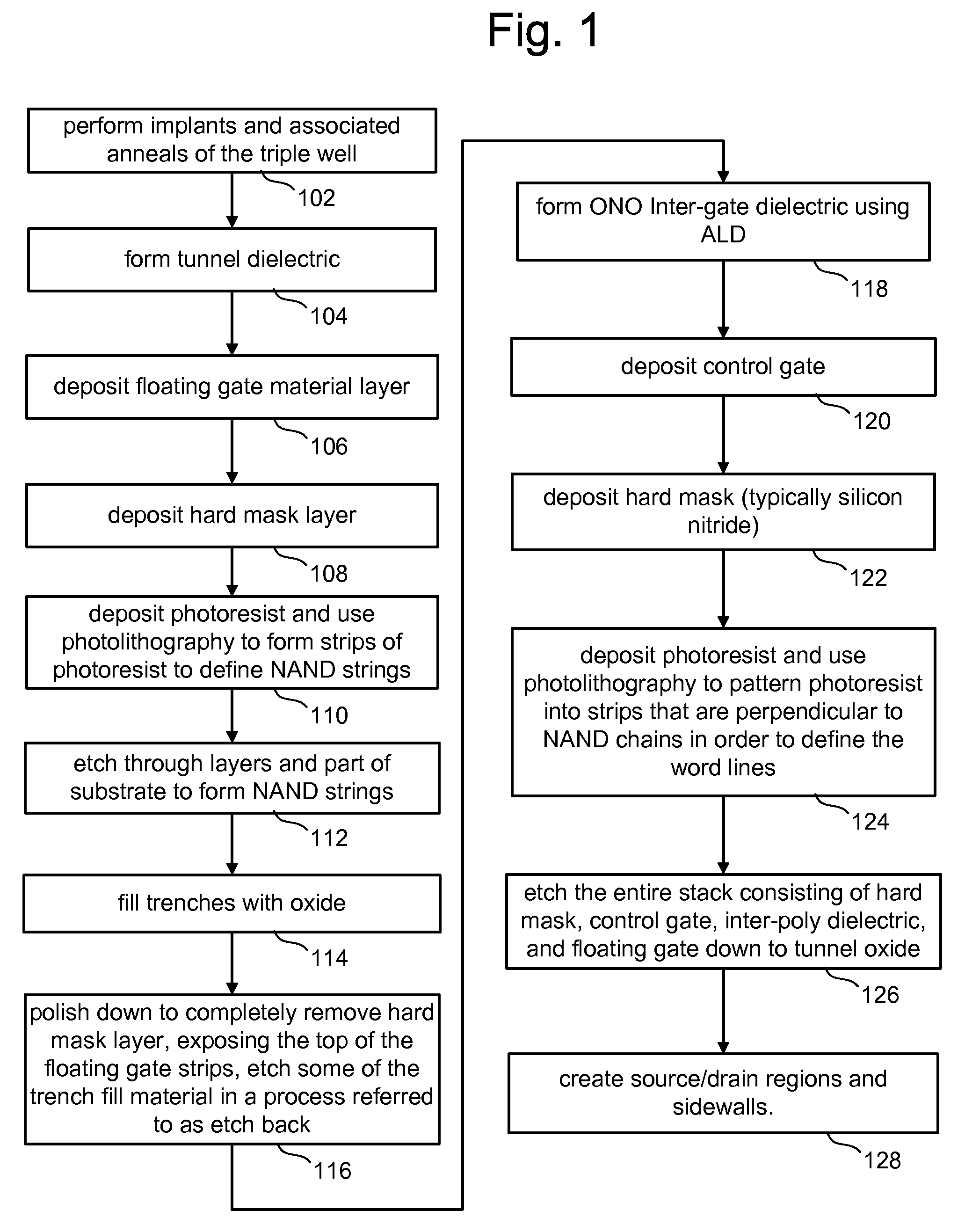
[0025]FIG. 1 is a flow chart describing one embodiment of the front end of a process for manufacturing a memory cell that describes the process steps as far as forming the sidewalls. This flow does not cover the optional booster plates or fins, the gap fill of etched volumes between the stacks, or forming the contacts, metallizations, vias, and passivation. While a flash memory will consist of both peripheral circuitry, which includes a variety of low, medium, and high voltage transistors, and the core memory array, the process steps of FIG. 1 are intended only to describe in general terms one possible process for the fabrication of the core memory array. Many photolithography, etch, implant, diffusion and oxidation steps that are intended for the fabrication of the peripheral transistors are omitted (but are known in the art).

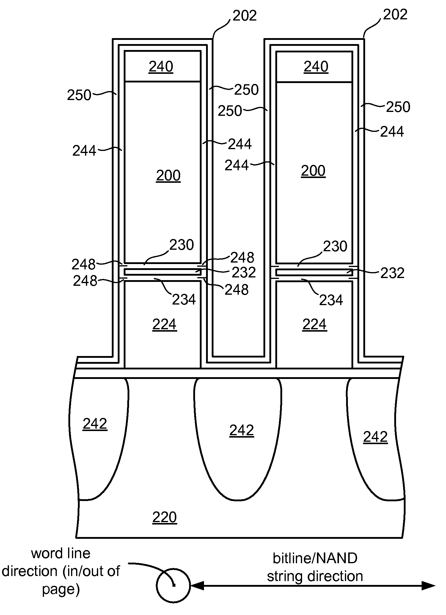
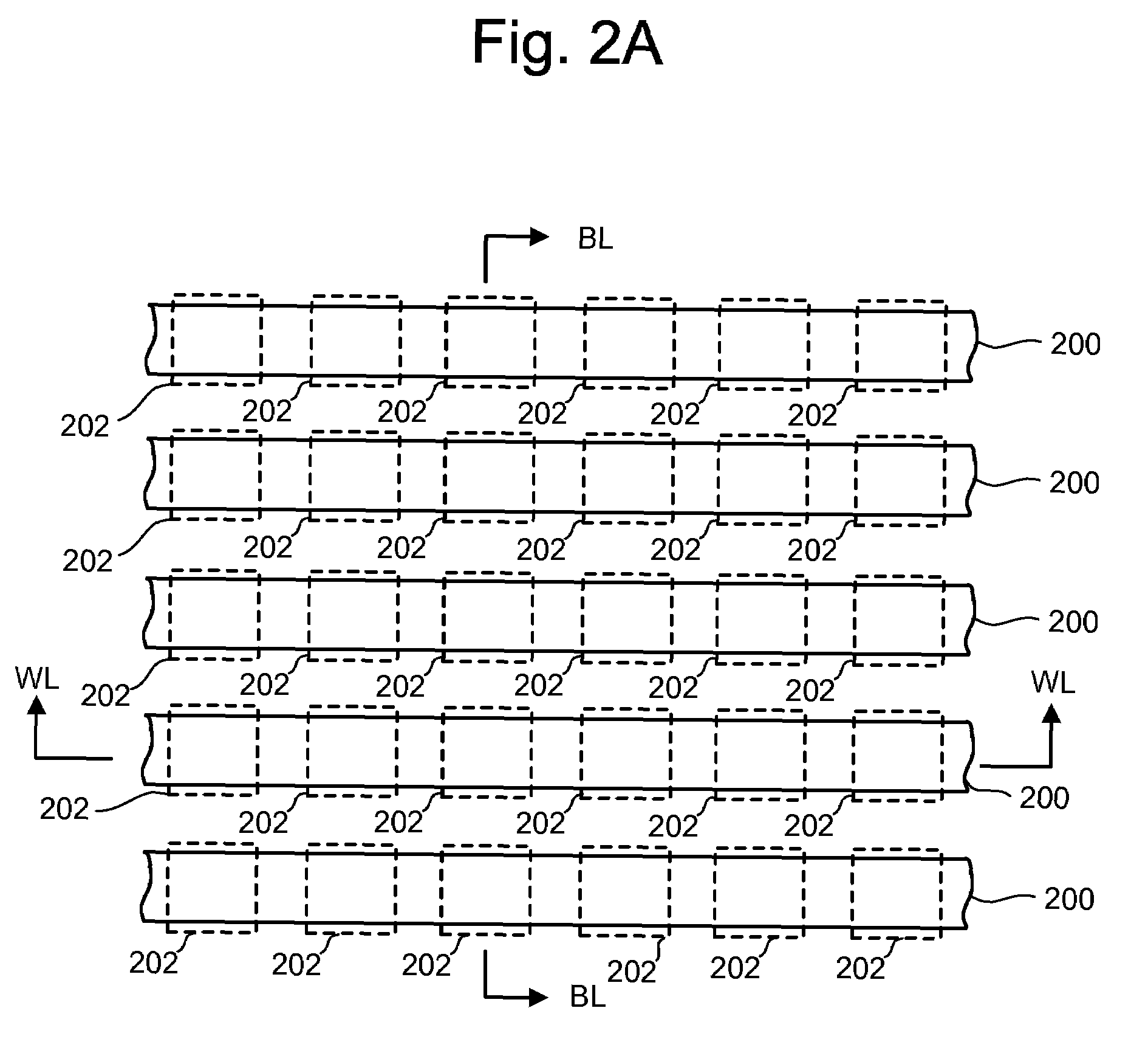
[0026]FIGS. 2A-2L will be used to explain the process of FIG. 1. FIG. 2A shows a top view of a portion of a memory array that includes floating gates 202 and ...


PUM


Abstract

Non-volatile storage elements (or other device) are created. One embodiment includes creating floating gate stacks comprising a floating gate, a control gate and a dielectric between the floating gate and the control gate. One example of a suitable dielectric includes a first layer of oxide, a layer of nitride and a second layer of oxide, all three of which are deposited using Atomic Layer Deposition (or other process). An implant (or other) process is used to create source/drain regions. ALD is used to deposit oxide and nitride for sidewalls.

Description

BACKGROUND OF THE INVENTION[0001]1. Field of the Invention[0002]The present invention relates to a non-volatile memory.[0003]2. Description of the Related Art[0004]Semiconductor memory devices have become more popular for use in various electronic devices. For example, non-volatile semiconductor memory is used in cellular telephones, digital cameras, personal digital assistants, mobile computing devices, non-mobile computing devices and other devices. Electrical Erasable Programmable Read Only Memory (EEPROM) and flash memory are among the most popular non-volatile semiconductor memories.[0005]Many types of EEPROM and flash memories utilize a floating gate that is positioned above and insulated from a channel region in a semiconductor substrate. The floating gate is positioned between source and drain regions. A control gate is provided over the floating gate. The control gate is insulated from the floating gate by a dielectric region. The threshold voltage of the transistor is cont...

Claims


Application Information

Patent Timeline
Patent Type & Authority Applications(United States)
IPC IPC(8): H01L21/336
CPCH01L21/28273H01L21/3144H01L29/513H01L27/11521H01L29/42324H01L27/115H01L29/40114H01L21/0228H01L21/0214H01L21/02148H01L21/022H01L21/02178H10B69/00H10B41/30
Inventor MOKHLESI, NIMA
Owner WODEN TECH INC
Why Eureka
Try Eureka