

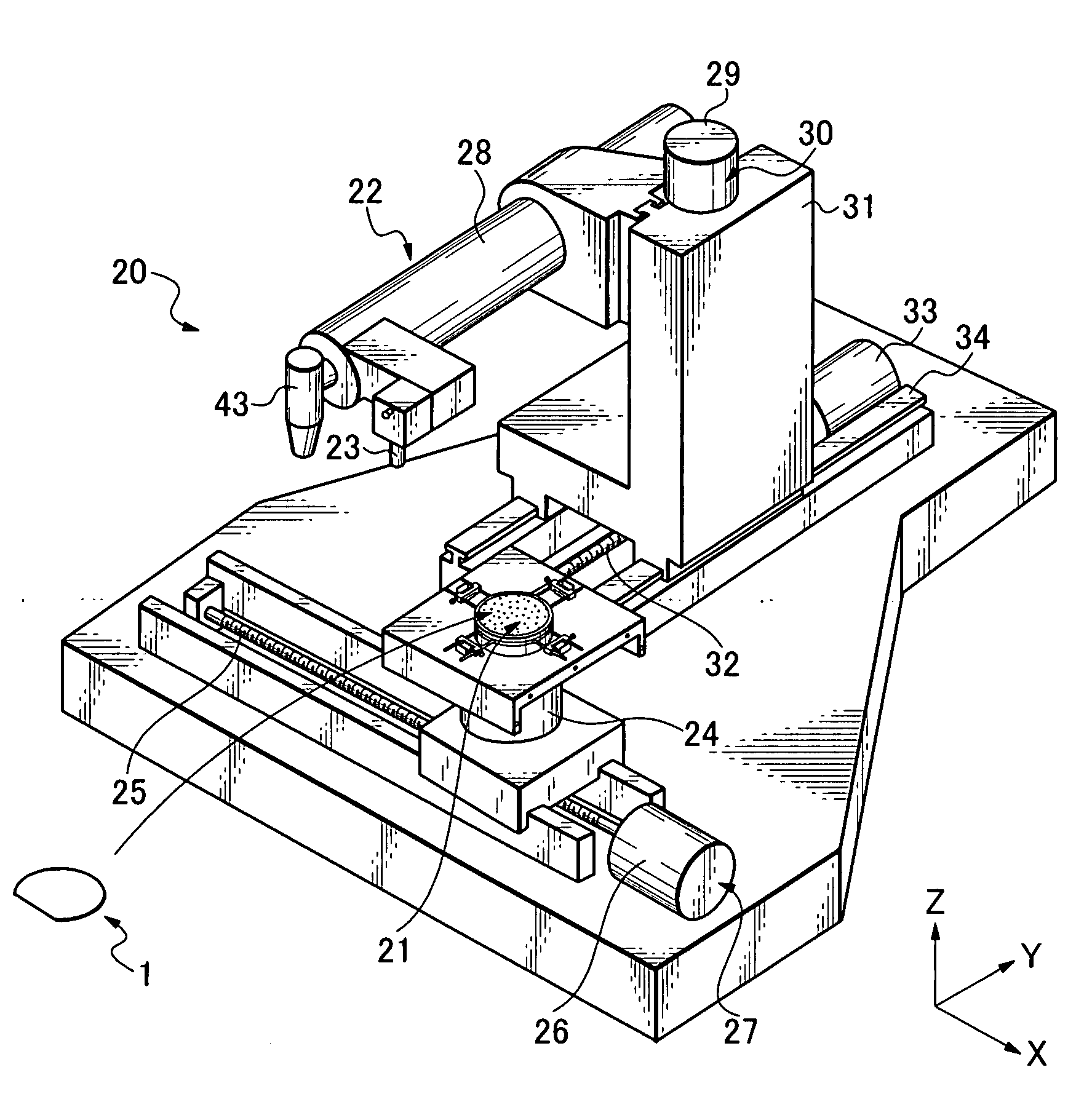
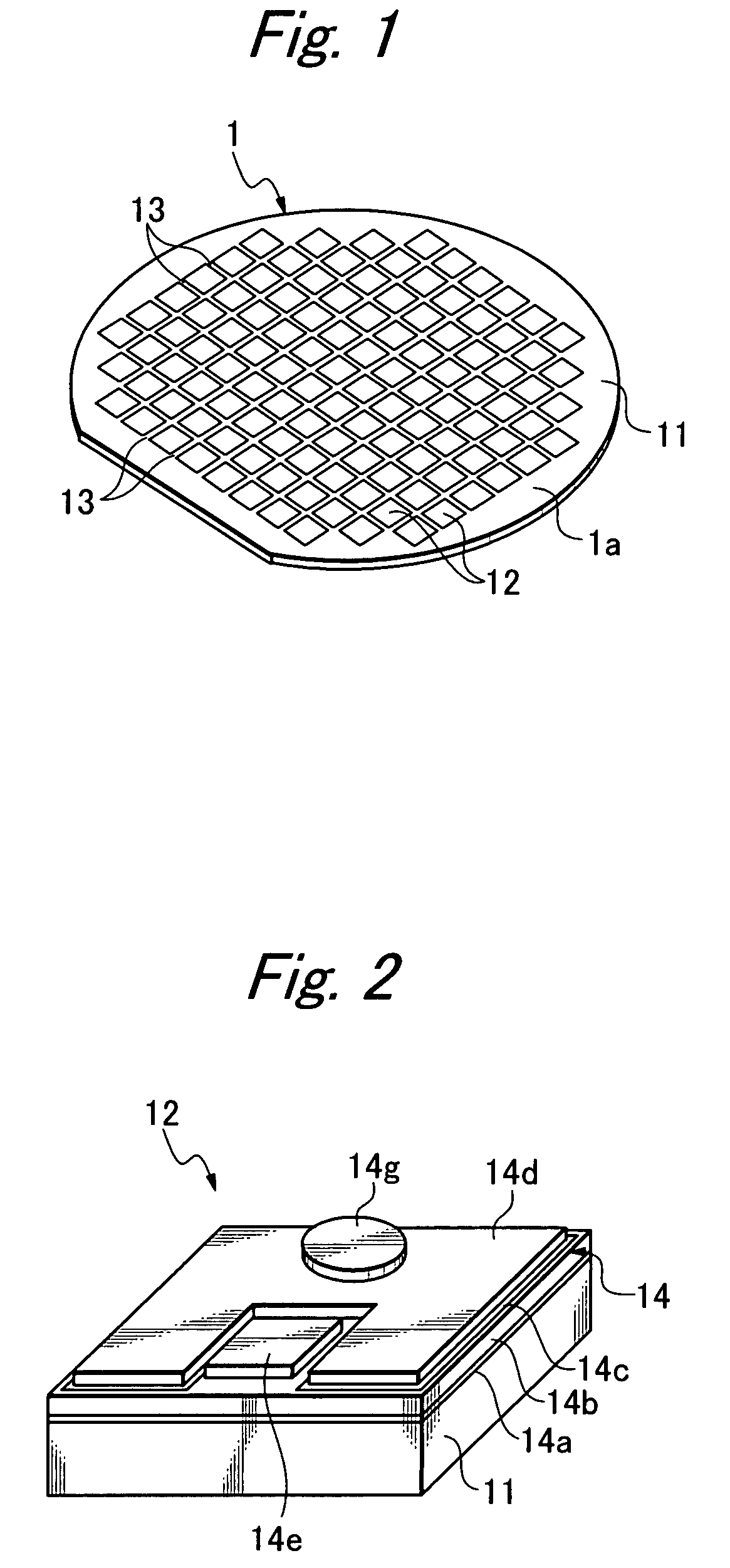
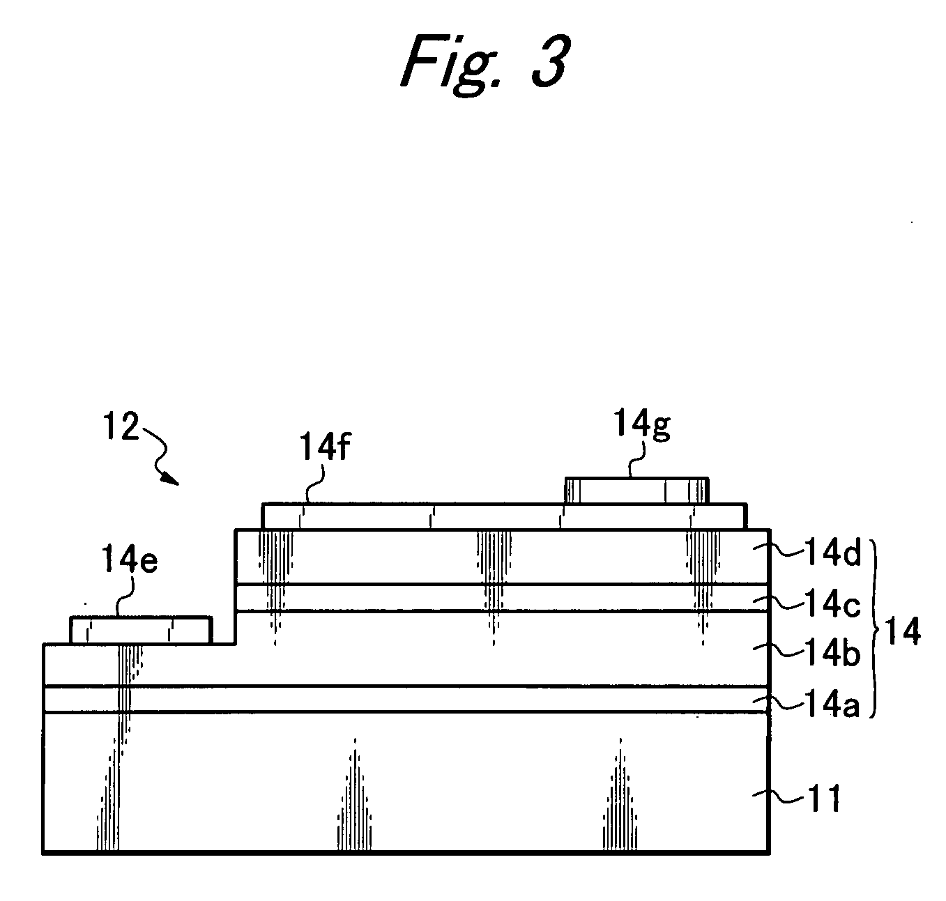
Method of processing sapphire substrate
- Summary
- Abstract
- Description
- Claims
- Application Information
AI Technical Summary
Benefits of technology
Problems solved by technology
Method used
Image

Examples
example 1
Wavelength: 1045 nm (Yb laser is used)
Average output 0.23 W
[0041]Repetition frequency: 100 kHz
Feed rate: 300 mm / s
Pulse width: 467 fs
Condensing spot size: about 0.9 μm
Pulse energy: 2.3 μJ
Pulse energy density: 360 J / cm2
Peak power density at condensing point P: 720 TW / cm2
example 2
Wavelength: 1560 nm (Er laser is used)
Average output 0.2 W
[0042]Repetition frequency: 100 kHz
Feed rate: 300 mm / s
Pulse width: 1000 fs
Condensing spot size: about 1.4 μm
Pulse energy: 2.0 μJ
Pulse energy density: 130 J / cm2
Peak power density at condensing point P: 130 TW / cm2
[0043]According to the processing condition as illustrated in the examples 1 or 2, a pulsed laser beam having a small pulse energy such as 2.3 μJ or 2.0 μJ, an extremely small pulse width in a range of femto-second such as 467 fs or 1000 fs, and high intensity is irradiated while the condensing point P is positioned within each of regions corresponding to the predetermined division lines 13 on the sapphire substrate 11 so that the affected zones 51 are formed, thereby the laser beam can be irradiated even at a high peak power density of 720 TW / cm2 or 130 TW / cm2, consequently each of the affected zones 51 can be formed at only a desired condensing point P within the sapphire substrate 11. Thus, a laser beam is transmi...
PUM
| Property | Measurement | Unit |
|---|---|---|
| Length | aaaaa | aaaaa |
| Length | aaaaa | aaaaa |
| Speed | aaaaa | aaaaa |
Abstract
Description
Claims
Application Information