Superfine-circuit semiconductor package structure

a semiconductor and superfine-circuit technology, applied in semiconductor devices, semiconductor/solid-state device details, electrical devices, etc., can solve the problems of limiting the height at which solder balls are disposed, lessening the routability of the substrate, and increasing the difficulty of wire bonding, so as to improve the reliability and simplify the process of conventional semiconductors , the effect of reducing costs

Inactive Publication Date: 2008-01-10
PHOENIX PRECISION TECH CORP
View PDF5 Cites 56 Cited by
  • Summary
  • Abstract
  • Description
  • Claims
  • Application Information

AI Technical Summary

Benefits of technology

[0008]In the light of the above-mentioned drawbacks of the prior art, it is a primary objective of the present invention to provide a superfine-circuit semiconductor package structure for combining a chip carrier manufacturing process with a chip packaging process with a view to meeting a flexibility need at client end and streamlining semiconductor processes and interface integration.
[0010]Yet another objective of the present invention is to provide a superfine-circuit semiconductor package structure for providing strong adherence between a circuit structure and an insulating layer with a view to maintaining a high level of process reliability.
[0011]A further objective of the present invention is to provide a superfine-circuit semiconductor package structure for efficiently dissipating heat generated by a semiconductor chip in operation, and providing electromagnetic shielding so as to minimize electromagnetic interference and noise interference from an external device.
[0012]A further objective of the present invention is to provide a superfine-circuit semiconductor package structure for solving the drawbacks of a conventional semiconductor packaging process, namely encapsulant spilling in a molding process, and layouts of conductive elements for a semiconductor chip, with a view to enhancing production quality and product reliability of a semiconductor device.
[0014]The superfine-circuit semiconductor package structure of the present invention combines a chip carrier (a circuit board) manufacturing process with a semiconductor chip packaging process with a view to streamlining the conventional semiconductor processes and interface integration. The superfine-circuit semiconductor package structure of the present invention streamlines a process and reduces costs by absolving a semiconductor process from wire bonding, a complicated flip chip related process, and process equipment required for electrical connection between a chip and a carrier structure thereof, which are otherwise necessary for the conventional semiconductor processes. The circuit built-up structure of the present invention uses a plurality of insulating layers such that openings configured for disposing the circuit layer is formed in the upper insulating layer and then vias penetrating the lower insulating layer is formed in the openings; in so doing, subsequently, the conductive vias are formed in the lower insulating layers, whereas the circuit layer is formed in the upper insulating layer. As a result, the circuit layer is perfectly affixed to the insulating layer so as to maintain a high level of reliability, and allow the circuit layer to be flush with the upper insulating layer such that the circuit built-up structures can be stacked on each other evenly. Accordingly, the objectives of a fine circuit manufacturing process are achieved.
[0015]The present invention provides at least one semiconductor chip mounted on a carrier board through a heat conduction adherence layer. Heat generated by the semiconductor chip in operation is efficiently dissipated. The carrier board, which is typically made of metal, efficiently provides electromagnetic shielding for the semiconductor device. The semiconductor chip is received in an through hole disposed in a metal board, an insulation board, or a circuit board mounted on the carrier board so as to reduce the overall thickness of the semiconductor device and thereby keep the semiconductor device small and compact. At least one stacking circuit structure is directly formed on the support board receiving the semiconductor chip so as to allow the semiconductor chip to electrically extend outward. At last, an edge of the stacking circuit structure is implanted with a plurality of conductive elements, such as solder balls, bonding pillars, and conductive pillars, so as to allow the package structure of the integrated chip to be electrically connected to an external device.

Problems solved by technology

Although the aforesaid package solves the problems of heat dissipation and shielding by means of the carrier board, it does have its own drawbacks.
In order to bond a solder ball to the printed circuit board smoothly, the solder ball is typically disposed at a height greater than the height of the loop of the corresponding wire, thus lessening the routability of the substrate and limiting the height at which the solder balls are disposed.
Owing to the densely distributed looped wires surrounding the chip, the wires are likely to touch each other and thereby result in shorting between the wires, making wire bonding increasingly difficult.
In practice, subject to the design of the semiconductor package, the package mold inevitably varies in dimensions and clamping / pressing positions and thereby cannot be tightly clamped and secured in position, and in consequence the encapsulant is likely to spill on the substrate surface, leading to two disadvantages: first, the semiconductor package surface is less likely to be even and esthetic; second, contamination may occur to a portion of the substrate formed with bond pads for implanting the solder balls, and thus compromising the quality of the electrical connection of the semiconductor package.
And further, during the filling process the resin material is a fluid, and mold fill pressure is exerted on the wire electrically connecting the chip and the substrate while the cavity is being filled with the resin material; in case of improper control over filling speed, the wires are prone to being swept by the mold flow, and in consequence the wires touch each other and result in short circuits, leading to deterioration of the quality and reliability of the semiconductor package.
However, the existing fine circuit technology is becoming less suitable for a semi-additive process; for instance, mass production of wires with line width and space rexpectively less than 10 μm by the existing fine circuit technology fails to achieve required dimension precision but incurs high costs.
In order to form a fine circuit structure perfectly affixed to an insulating layer, the insulating layer must have a smooth, even surface before the formation of the fine circuit structure thereon, otherwise circuit layers subsequently disposed on the insulating layer is likely to peel off, ending up with deteriorated reliability.
In practice, the uneven surface of the inner-layer patterned circuit formed in the substrate inevitably causes the surface of the insulating layer disposed on the substrate to be uneven.
Similarly, the built-up circuit layers formed on the insulating layer having the uneven surface cannot be perfectly affixed to the insulating layer because of the uneven surface of the insulating layer but may even peel off.
The smaller the boundary surface between the built-up circuit layers and the insulating layer is, the more serious is the aforesaid phenomenon associated with formation of a fine circuit structure.
The processes involve various process manufacturers (including chip carrier manufacturers and semiconductor package manufacturers), and thus the fabrication process not only comprises complicated steps but also uses incompatible interfaces.
And further, if the client end intends to change a function or a design, the involved change and the required integration will be extremely intricate.
Accordingly, the fabrication process fails to be flexible, and cost-efficient.

Method used


Image

  • Superfine-circuit semiconductor package structure
  • Superfine-circuit semiconductor package structure
  • Superfine-circuit semiconductor package structure

Examples


Embodiment Construction

[0021]The following specific embodiments are provided to illustrate the disclosure of the present invention, these and other advantages and effects can be apparently understood by those skilled in the art after reading the disclosure of this specification. The present invention can also be performed or applied by other different embodiments. The details of the specification may be modified or changed on the basis of different points and applications without departing from the spirit of the present invention.

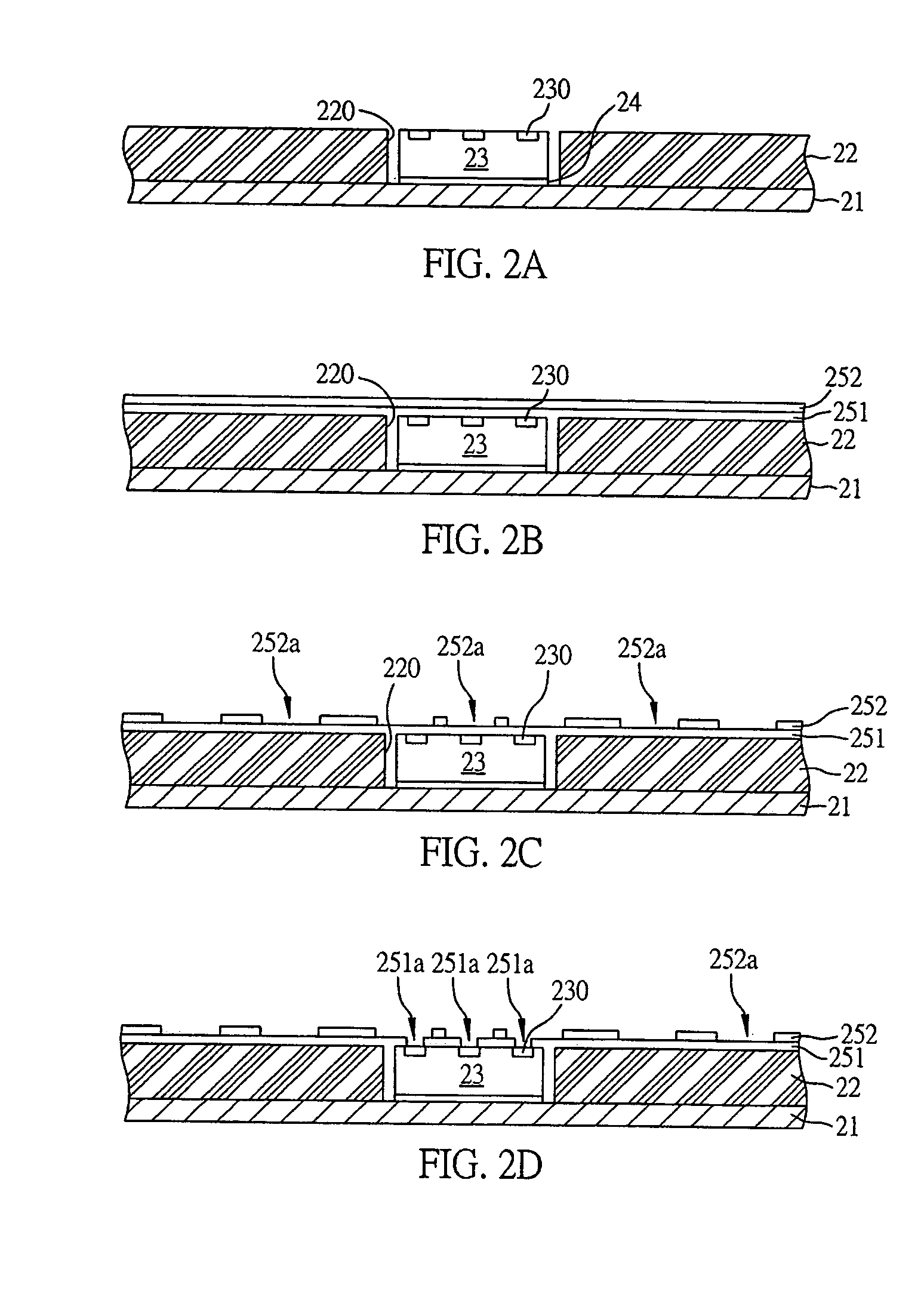
[0022]FIGS. 2A to 2H are cross-sectional schematic diagrams showing how to fabricate a superfine-circuit semiconductor package structure in accordance with the present invention.

[0023]As shown in FIG. 2A, the present invention provides a carrier board 21 on which a support board 22 with a through hole 220 is mounted. At least one semiconductor chip 23 is mounted on the carrier board 21 and received in the through hole 220 of the support board 22. The support board 22 is one selec...


PUM


Abstract

A superfine-circuit semiconductor package structure includes a carrier board, a support board having at least one through hole and mounted on the carrier board, at least one semiconductor chip received in the through hole of the support board and mounted on the carrier board, at least one circuit built-up structure electrically connected to the semiconductor chip and formed on the support board and the semiconductor chip, wherein the circuit built-up structure includes at least two insulating layers, a plurality of conductive vias formed in the lower insulating layer, circuit layer electrically connected to the conductive vias and flush with the upper insulating layer, and a plurality of conductive elements mounted on the circuit built-up structure, such that the semiconductor chip can be electrically connected to an external device through the circuit built-up structure and the conductive elements.

Description

CROSS-REFERENCE TO RELATED APPLICATION[0001]This application claims benefit under 35 USC 119 of Taiwan Application No. 094100802, filed Jan. 12, 2005.FIELD OF THE INVENTION[0002]The present invention relates to a superfine-circuit semiconductor package structure, and more particularly, to a superfine-circuit semiconductor package structure that combines a carrier board, a semiconductor chip, and a circuit structure.BACKGROUND OF THE INVENTION[0003]Development of semiconductor package technology brings a variety of semiconductor packages. For instance, Ball Grid Array (BGA) packaging, which represents an advanced semiconductor packaging technology, involves mounting a semiconductor chip on a substrate, implanting a grid-like array of solder balls on the bottom of the substrate by self-alignment, and forming electrical and mechanical bridges between the package and the printed circuit board by means of the solder balls; in so doing, relatively more I / O connections are disposed on a se...

Claims


Application Information

Patent Timeline
Patent Type & Authority Applications(United States)
IPC IPC(8): H01L23/12
CPCH01L23/5389H01L2224/0401H01L24/24H01L2224/04105H01L2224/20H01L2224/24227H01L2224/48091H01L2224/73265H01L2224/73267H01L2924/01012H01L2924/01013H01L2924/01029H01L2924/01082H01L2924/15153H01L2924/1517H01L2924/15311H01L2924/3025H01L24/19H01L2224/92244H01L2224/32225H01L2224/12105H01L2924/01087H01L2924/01033H01L24/48H01L2924/01006H01L2924/00015H01L2924/00014H01L2924/181H01L2924/00012H01L2224/45099H01L2224/45015H01L2924/207
Inventor HSU, SHIH-PING
Owner PHOENIX PRECISION TECH CORP
Why Eureka
Try Eureka