Treatment for bonding interface stabilization

a stabilization treatment and bonding technology, applied in the direction of basic electric elements, semiconductor/solid-state device manufacturing, electric devices, etc., can solve the problems of insufficient stabilization of the bonding interface, partial solutions including long-duration stabilization annealing to stabilize the bonding interface are not completely satisfactory, and the thin layer of the donor material may not support furnace stabilization annealing for several hours, etc., to achieve the effect of facilitating the bonding of the donor substra

Active Publication Date: 2008-01-17
S O I TEC SILICON ON INSULATOR THECHNOLOGIES
View PDF9 Cites 17 Cited by
  • Summary
  • Abstract
  • Description
  • Claims
  • Application Information

AI Technical Summary

Benefits of technology

[0019]In accordance with a further aspect of the invention, the method may further include exposing at least one of (i) an exposed face of the donor substrate and (ii) an exposed face of a support substrate to plasma to facilitate bonding of the donor substrate to the support substrate prior to the bonding step. The duration of exposure to plasma may be between about 5 seconds and about 60 seconds, preferably about 30 seconds. In accordance with one embodiment, the plasma includes at least one gaseous constituent selected from the group including Oxygen, Nitrogen, Helium, Argon, and mixtures thereof, among others. The gaseous constituent is preferably introduced into a reaction chamber containing the silicon structure at a rate of flow between about 50 sccm and about 500 sccm. In accordance with a further aspect, the gaseous constituent may be introduced into a reaction chamber to establish a mean gaseous pressure within the chamber between about 10 mTorr and about 200 mTorr, preferably about 50 mTorr. The plasma may be initiated and maintained by application of a radiofrequency power per unit of surface area of the surface to be treated in an amount between about 150 mW/cm2 and about 2800 mW/cm2, preferably about 750 mW/cm2. For example, the plasma may be initiated and maintaine...

Problems solved by technology

However, previous solutions do not allow the bonding interface to be sufficiently stabilized.
However, these partial solutions including long-duration stabilization annealing to stabilize the bonding interface is not completely satisfactory.
First, the thin layer from the donor material may not support furnace stabilization annealing for several hours.
For example, such annealing applied to a thin strained silicon layer is likely to generate dislocation type defects in the thickness of the thin layer and to consequently result in relaxation of the constrained material.
Second, stabilization annealing is a long operation, typically taking several hours.
This requires a significant heat budget.
Also, stabilization annealing complicates the manufac...

Method used


Image

  • Treatment for bonding interface stabilization
  • Treatment for bonding interface stabilization
  • Treatment for bonding interface stabilization

Examples


first embodiment

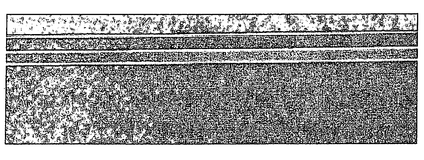
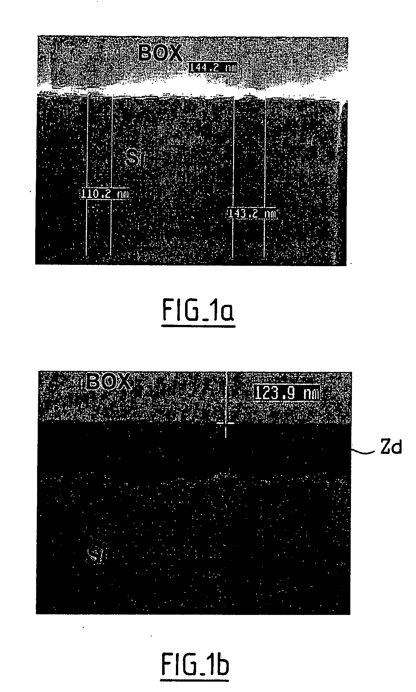
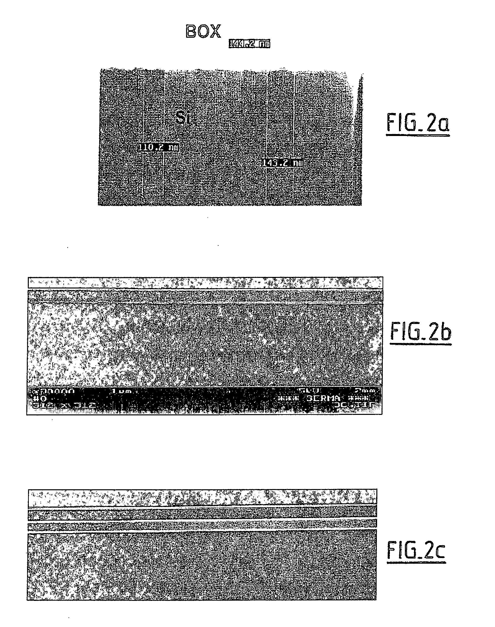
[0048]In the scope of a preferential variation of this first embodiment, the thin layer thinning step is carried out between each RTA operation. Thinning may be carried out by the implementation of thermal oxidation at a temperature of less than or equal to 1000° C. followed by desoxidation as described above.

[0049]In accordance with another embodiment of the invention, the stabilization annealing step may be replaced by performing a bonding energy reinforcement step carried out before detachment, and a stabilization step for the bonding interface carried out by implementing one or more rapid thermal annealing operations after detachment.

second embodiment

[0050]For purposes of illustration and not limitation, as embodied herein, the bonding energy reinforcement step may be implemented before bonding and preferably includes a plasma treatment of one and / or the other of the surfaces to be bonded. Specifically, in the scope of this second embodiment, the donor substrate (oxidized or not oxidized in such a way as to form an oxide layer used as the insulating layer inserted between the thin layer and the support substrate) and / or the donor substrate (oxidized or not oxidized for the same reasons) is (are) exposed to plasma, before close contact with the faces to be bonded.

[0051]The duration of exposure to plasma is between 5 and 60 seconds; it typically is approximately 30 seconds. Equipment conventionally utilized in microelectronics to perform dry etching may be utilized in order to implement this plasma treatment step. In particular, this is equipment allowing RIE (Reactive Ion Etching) type etching to be carried out. Suitable equipmen...


PUM


Abstract

A method and/or system are provided for producing a structure comprising a thin layer of semiconductor material on a substrate. The method includes creating an area of embrittlement in the thickness of a donor substrate, bonding the donor substrate with a support substrate and detaching the donor substrate at the level of the area of embrittlement to transfer a thin layer of the donor substrate onto the support substrate. The method also includes thermal treatment of this resulting structure to stabilize the bonding interface between the thin layer and the substrate support. The invention also relates to the structures obtained by such a process.

Description

CROSS-REFERENCE TO RELATED APPLICATION[0001]This application claims the benefit of priority from U.S. patent application Serial Ser. No. 11 / 788,292, filed Apr. 19, 2007 and from French Patent Application Serial No. FR0606440 filed Jul. 13, 2006. The disclosure of each of these applications is incorporated by reference herein in its entirety.BACKGROUND OF THE INVENTION[0002]1. Field of the Invention[0003]The present invention relates to a method and system for processing silicon materials. Particularly, the present invention is directed to a method and system for providing a thin layer of semiconductor material on a substrate and the resulting structure.[0004]2. Description of Related Art[0005]A variety of methods and systems are known in the art for providing a thin layer of semiconductor material on a substrate. Such methods and systems include, for example, Smart Cut™ type methods. Details concerning the Smart Cut™ method can be found in the document, “Silicon-on-Insulator Technol...

Claims


Application Information

Patent Timeline
IPC IPC(8): H01L21/30
CPCH01L21/76254H01L21/324H01L21/477
Inventor NEYRET, ERICKERDILES, SEBASTIEN
Owner S O I TEC SILICON ON INSULATOR THECHNOLOGIES
Why Eureka
Try Eureka